Method and System of Linking On-Chip Parasitic Coupling Capacitance Into Distributed Pre-Layout Passive Models

Inactive Publication Date: 2010-12-30
GLOBALFOUNDRIES INC
View PDF11 Cites 1 Cited by
  • Summary
  • Abstract
  • Description
  • Claims
  • Application Information

AI Technical Summary

Benefits of technology

[0008]According to the exemplary embodiment detailed above, a method for modeling on-chip parasitic coupling capacitance in a distributed passive model allows pre-layout passive models to accurately include post-layout parasitics. Accuracy of transmission line modeling may

Problems solved by technology

This causes inaccuracies because of an overestimation of the capacitance.
Thus, conventionally, there is no way to model on-chip layout parasitic capacitance interactions

Method used


Image

  • Method and System of Linking On-Chip Parasitic Coupling Capacitance Into Distributed Pre-Layout Passive Models
  • Method and System of Linking On-Chip Parasitic Coupling Capacitance Into Distributed Pre-Layout Passive Models
  • Method and System of Linking On-Chip Parasitic Coupling Capacitance Into Distributed Pre-Layout Passive Models

Examples


Example

[0016]It will be appreciated that for simplicity and clarity of illustration, elements shown in the figures have not necessarily been drawn to scale. For example, the dimensions of some of the elements may be exaggerated relative to other elements for clarity. Further, where considered appropriate, reference numbers may be repeated among the figures to indicate corresponding or analogous features.

DETAILED DESCRIPTION OF THE INVENTION

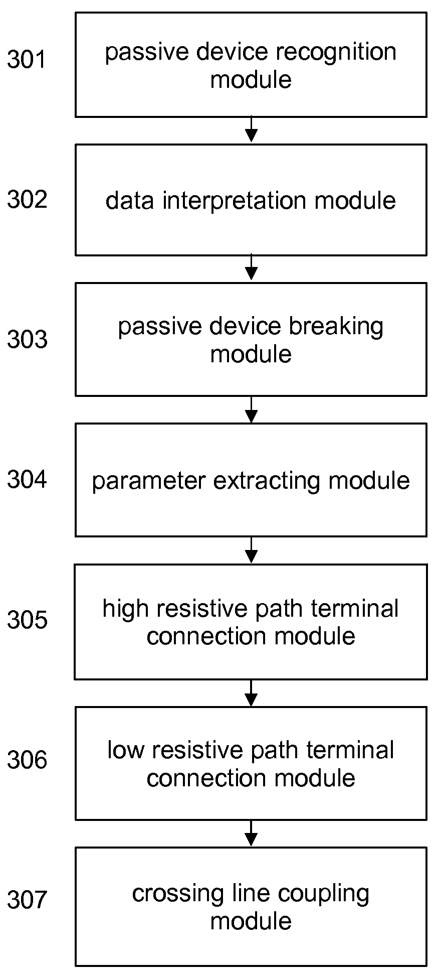
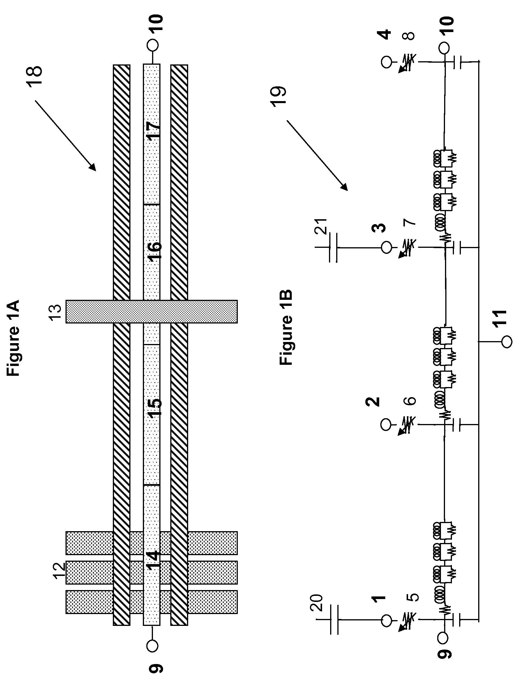
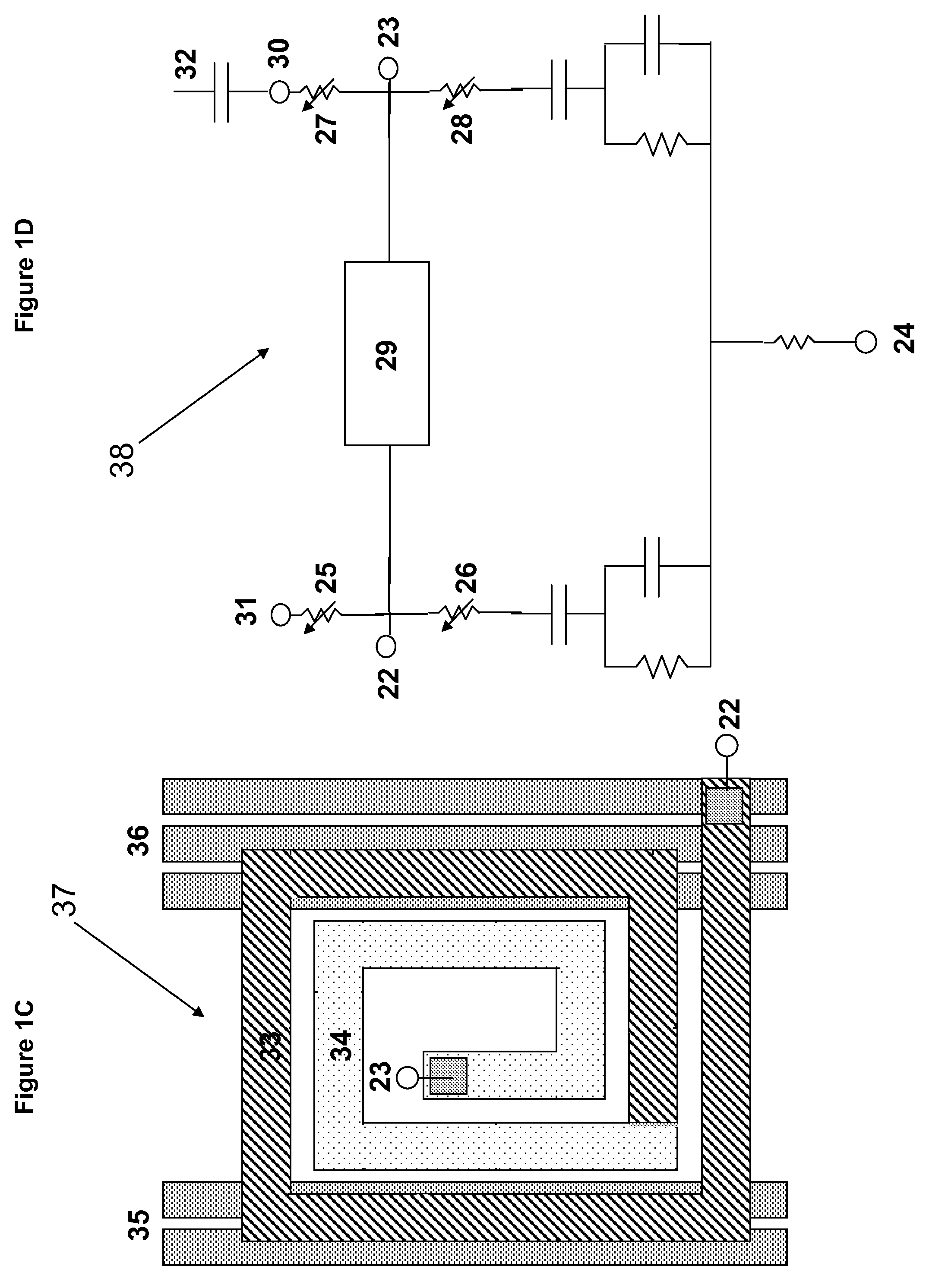
[0017]Referring now to the drawings, and more particularly to FIGS. 1-3, there are shown exemplary embodiments of the structures and method according to the present invention.

[0018]FIGS. 1A and 1B show exemplary embodiments of the layout design and the simulation netlist, respectively, of the single CPW netlist of the present invention for linking to parasitic extraction tools in relation to t-lines showing cross-under and cross-over lines.

[0019]FIG. 1A is an exemplary illustration of how a CPW is designed according to the present invention. Reference nu...


PUM


Abstract

A method of linking on-chip parasitic coupling capacitance into distributed pre-layout passive models such as distributed transmission line models and on-chip spiral inductor models includes recognizing a passive device such as a distributed transmission line device and an on-chip spiral inductor device, interpreting data obtained from the recognizing the passive device, breaking the passive device into a plurality of sections, the plurality of sections including a terminal of a model call, extracting parameters of the passive device by Layout Versus Schematic (LVS) and parasitic extraction, connecting the terminal to a pre-layout passive network by selectively low and high resistive paths set by the parameters of the passive device depending on whether crossing lines are present or not present in one of the plurality of sections, connecting the terminal to a distributed passive model, and coupling the crossing lines to the terminal via capacitors produced in an extracted netlist with the passive device having distributed coupling to a plurality of crossing lines.

Description

BACKGROUND OF THE INVENTION[0001]The present invention relates generally to a method and system of linking on-chip parasitic coupling capacitance into distributed pre-layout passive models. In particular, the present invention relates to a method and system of linking on-chip parasitic coupling capacitance into distributed pre-layout passive models such as transmission lines and on-chip spiral inductors that accurately does so in a physically realistic manner.[0002]On-chip passive models such as transmission lines (t-lines) are used for fast and accurate pre-layout estimation of high-frequency, critical interconnect configurations. A P-Cell draws the t-line layout and, through marker shapes, the Layout Versus Schematic (LVS) recognizes the t-line and calls the t-line “compact model”. The LVS blocks parasitic extraction from extracting the capacitance, resistance, and inductance of the t-line metals.[0003]In the case of t-lines, conventionally, the parasitic networks of neighboring c...

Claims


Application Information

Patent Timeline
IPC IPC(8): G06F17/50
CPCG06F17/5036G06F30/367
Inventor WOODS, WAYNE H.ZEMKE, COLE E.
Owner GLOBALFOUNDRIES INC
Why Eureka
Try Eureka