Field-effect transistor, single-electron transistor and sensor using the same

a single-electron transistor and field-effect technology, applied in the field of field-effect transistors, single-electron transistors and sensors using the same, can solve problems that have not yet been realized, and achieve the effect of high detection sensitivity

Inactive Publication Date: 2007-03-22
JAPAN SCI & TECH CORP
View PDF10 Cites 63 Cited by
  • Summary
  • Abstract
  • Description
  • Claims
  • Application Information

AI Technical Summary

Benefits of technology

[0040] According to the sensor of the present invention, it is ...

Problems solved by technology

Therefore, it has not yet realized because of its ...

Method used


Image

  • Field-effect transistor, single-electron transistor and sensor using the same
  • Field-effect transistor, single-electron transistor and sensor using the same
  • Field-effect transistor, single-electron transistor and sensor using the same

Examples


first embodiment

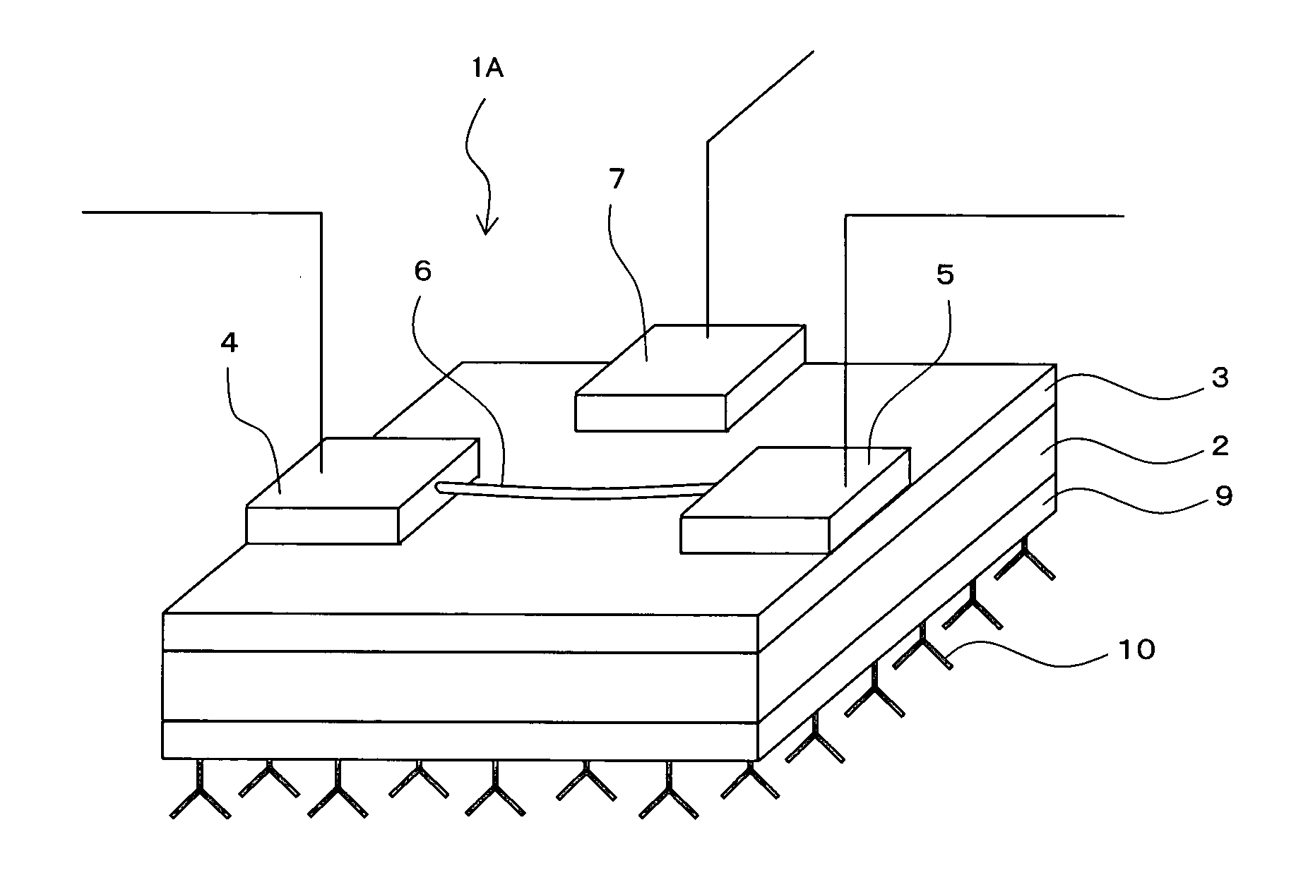
[0079]FIG. 1 (a) and FIG. 1 (b) illustrate sensors according to a first embodiment of the present invention. As shown in FIG. 1 (a), the substrate 2 of the transistor 1A is made of insulating material. On the upside (upper side in the FIGS.) of the entire substrate, the silicon oxide layer of insulating and low-permittivity material (hereinafter, called “low-permittivity layer,” if necessary) 3 is formed. On the right side of the low-permittivity layer 3, the source electrode 4 and the drain electrode 5, formed of gold, are placed, between which the channel 6 formed with a carbon nano tube is bridged.

[0080] The channel 6 is bridged between the source electrode 4 and the drain electrode 5 as if it were a bridge that connects the source electrode 4 and the drain electrode 5. Thereby it is apart from the low-permittivity layer 3 and the channel 6 is fixed to the transistor 1A at its two connecting points with the source electrode 4 and the drain electrode 5. The other portion of the c...

second embodiment

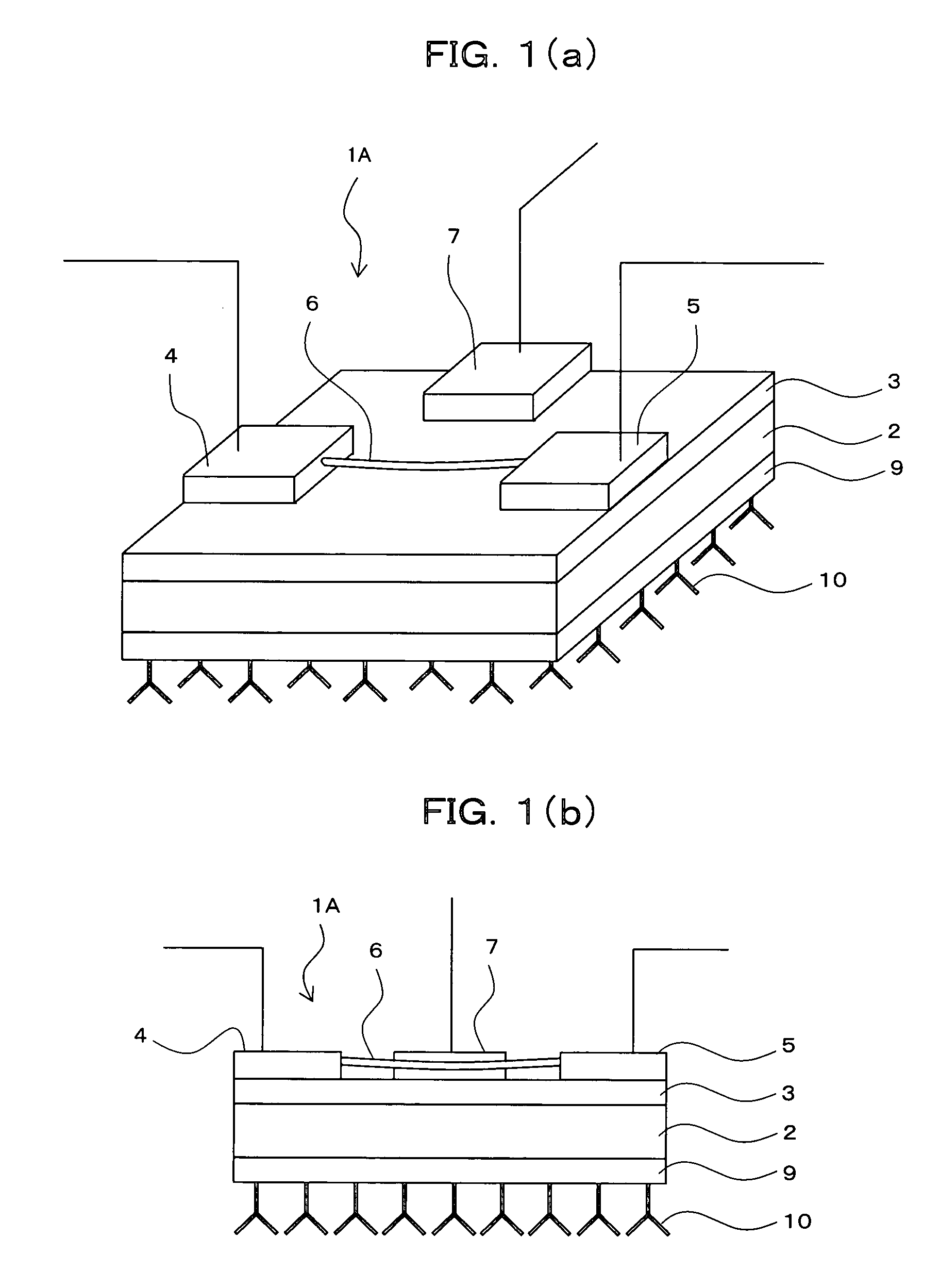
[0096]FIG. 2 (a) and FIG. 2 (b) illustrate sensors according to a second embodiment of the present invention. As shown in FIG. 2 (a), the transistor 1B constructing the sensor of the second embodiment of the present invention has similar structure to the transistor 1A described in the first embodiment.

[0097] The transistor 1B of the present embodiment further comprises the photosensitive resin layer of insulating and high-permittivity material (hereinafter, called “high-permittivity layer,” if necessary) 11 is formed on the upside of the entire low-permittivity layer 3. The high-permittivity layer 11 is formed to cover the whole channel 6, the lateral sides of the source electrode 4, the drain electrode 5 and the side gate 7 but not to cover the upsides (upper sides in FIGS.) of the source electrode 4, the drain electrode 5 and the side gate 7. The high-permittivity layer 11 is shown by chain double-dashed line in FIG. 2 (a) and FIG. 2 (b).

[0098] Because the sensor of the present ...

third embodiment

[0104]FIG. 3 (a) and FIG. 3 (b) illustrate sensors according to the third embodiment of the present invention. As shown in FIG. 3 (a), the transistor 1C constructing the sensors according to this embodiment, similar to the first embodiment, comprises the substrate 2 fabricated with insulating material, the insulating and low-permittivity layer 3, the source electrode 4 and the drain electrode 5. The source electrode 4 and the drain electrode 5 are formed with gold. The channel 6 formed with a carbon nano tube is brdged between the source electrode 4 and the drain electrode 5.

[0105] The back gate 12 for applying a gate voltage to the transistor 1C is formed on the back side of entire substrate 2. The back gate 12 is connected to a power supply, not shown in FIGS., which applies a voltage to the back gate 12. The voltage placed to the back gate 12 is able to be measured with a measuring instrument, not shown in FIGS.

[0106] The membrane fabricated with silicon oxide (insulating membr...


PUM


Abstract

A sensor capable of detecting detection targets that are necessary to be detected with high sensitivity is provided.
It comprises a field-effect transistor 1A having a substrate 2, a source electrode 4 and a drain electrode 5 provided on said substrate 2, and a channel 6 forming a current path between said source electrode 4 and said drain electrode 5;
wherein said field-effect transistor 1A comprises:
an interaction-sensing gate 9 for immobilizing thereon a specific substance 10 that is capable of selectively interacting with the detection targets; and
a gate 7 applied a voltage thereto so as to detect the interaction by the change of the characteristic of said field-effect transistor 1A.

Description

TECHNICAL FIELD [0001] The present invention relates to a field-effect transistor, a single-electron transistor and a sensor using the same. BACKGROUND ART [0002] A field-effect transistor (FET) and a single-electron transistor (SET) are elements that convert voltage signals input in a gate into current signals output from either a source electrode or a drain electrode. On placing a voltage between the source electrode and the drain electrode, charged particles exsiting in the channel move between the source electrode and the drain electrode along the direction of electric field and are output from either the source electrode or the drain electrode as a current signal. [0003] At this point, the strength of the output current signal is proportional to the density of the charged particles. When a voltage is applied on the gate that is placed at upward, sideward or downward position of the channel with an insulator therebetween, the density of the charged particles exsiting in the chan...

Claims


Application Information

Patent Timeline
IPC IPC(8): H01L31/06B82Y10/00B82Y15/00B82Y35/00G01N27/00G01N27/414H01L29/06H01L29/66H01L29/80
CPCB82Y10/00G01N27/4146G01N27/4145B82Y30/00B82Y40/00H01L21/18H01L29/068H01L29/42364H01L29/7613
Inventor MATSUMOTO, KAZUHIKOKOJIMA, ATSUHIKONAGAO, SATORUKATOU, MASANORIYAMADA, YUTAKANAGAIKE, KAZUHIROIFUKU, YASUOMITANI, HIROSHI
Owner JAPAN SCI & TECH CORP
Why Eureka
Try Eureka