Avalanche quantum intersubband transition semiconductor laser

a semiconductor laser and quantum intersubband technology, applied in the field of quantum intersubband transition semiconductor lasers, can solve the problem that the wavelength band cannot be obtained with a conventional semiconductor laser diode, and achieve the effect of simple compact structure and easy manufacturing

Inactive Publication Date: 2007-03-22
ELECTRONICS & TELECOMM RES INST
View PDF10 Cites 2 Cited by
  • Summary
  • Abstract
  • Description
  • Claims
  • Application Information

AI Technical Summary

Benefits of technology

[0014] The present invention is directed to implementation of an quantum intersubband transition semiconductor lase

Problems solved by technology

This wavelength band cannot be obtained with a conventional semiconductor laser diode.
Accordingly, since the complicated multi layer should be epitaxially grown by a molecular bea

Method used


Image

  • Avalanche quantum intersubband transition semiconductor laser
  • Avalanche quantum intersubband transition semiconductor laser
  • Avalanche quantum intersubband transition semiconductor laser

Examples


Embodiment Construction

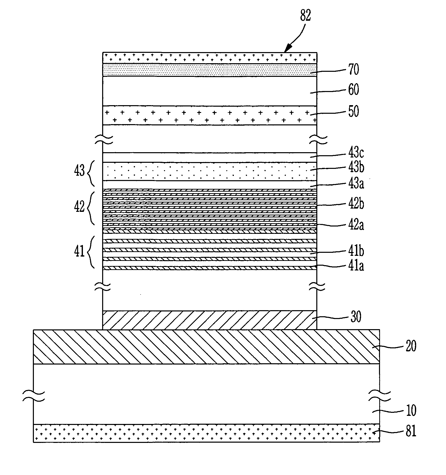
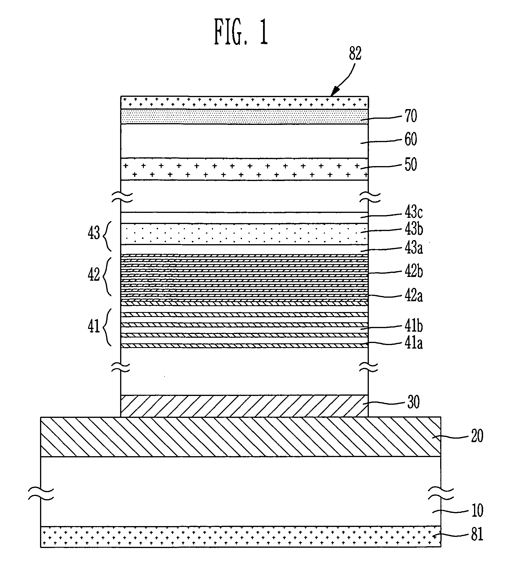
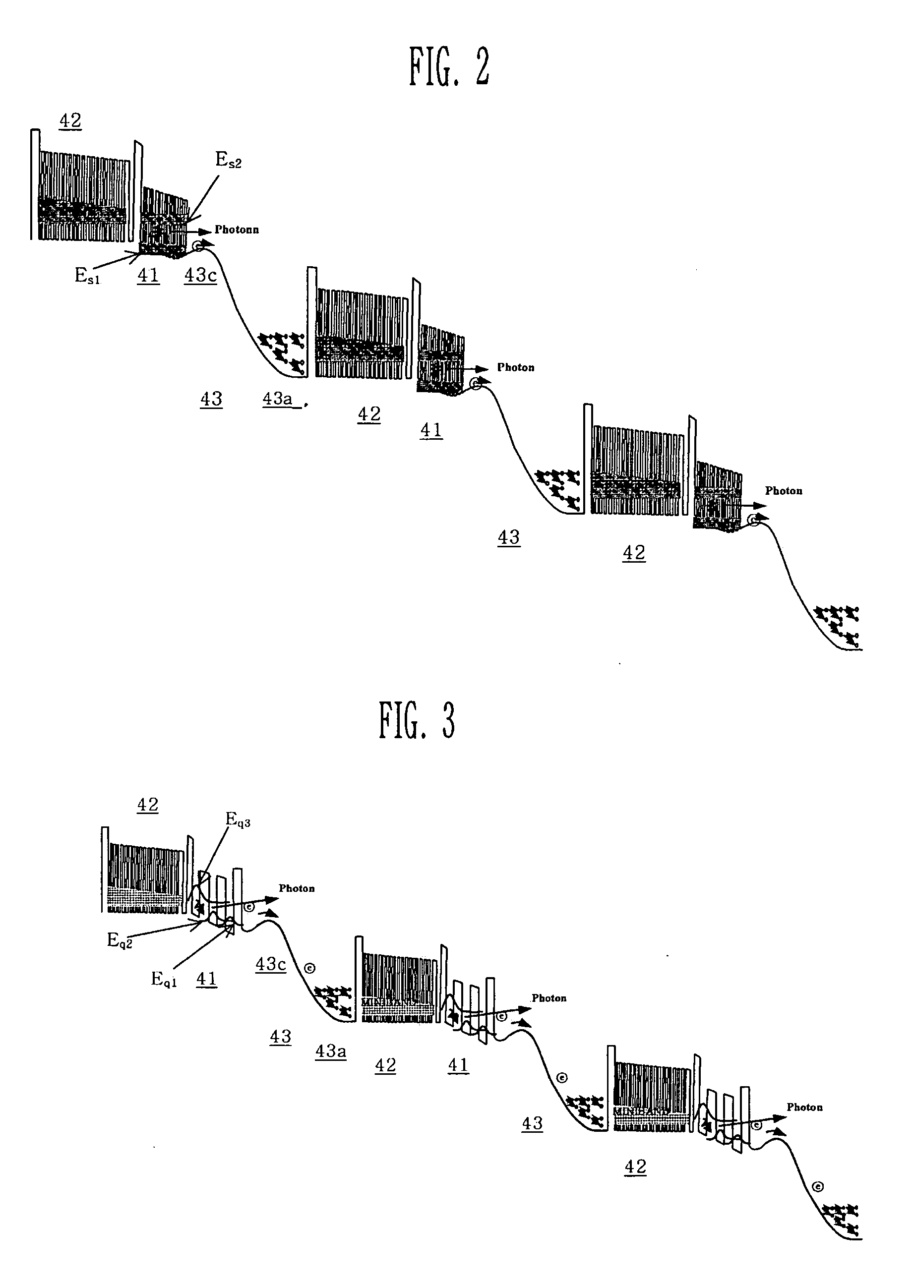
[0025] Since a conventional mid / far infrared quantum cascade laser has a structure where one electron passes through N stacks (periods) of unit-cell structure while emitting N photons, it needs stacks (periods) of 25 to 70 or more in number so as to obtain sufficient optical power. Accordingly, the structure is complicated, difficult in growing a quantum cascade laser structure.

[0026] The present invention forms a carrier-multiplication layer structure including PIN type layers for generating carrier multiplication between QW active regions in which an intersubband radiative transition occurs, and a carrier guide layer structure structure for relaxing energies of multiplied carriers and injecting multiplied carriers into an upper transition level of an adjacent QW active region. The present invention enhances efficiency of carrier injection into the QW active region to achieve high population inversion, thereby obtaining high power even with a simple compact stacks (periods) and th...


PUM


Abstract

Provided is an avalanche quantum intersubband transition semiconductor laser. The laser includes: a first cladding layer, a first wave guide layer, an active region, a second wave guide layer, and a second cladding layer formed on a semiconductor substrate, wherein the active region consists of multiple stacks (periods) of a unit-cell structure, which is comprised of a carrier-multiplication layer structure for multiplying carriers, a carrier guide layer structure, and an QW active region to which carriers are injected, wherein intersubband optical radiative transitions of the carriers occur. Here, the carriers multiplied while passing though the carrier-multiplication layer structure, and injected into a optical transition level of the QW active region can achieve the high population inversion effectively, thereby high laser output power can be obtained with less stacked compact structure.

Description

CROSS-REFERENCE TO RELATED APPLICATION [0001] This application claims priority to and the benefit of Korean Patent Application No. 2005-67857, filed Jul. 26, 2005, the disclosure of which is incorporated herein by reference in its entirety. BACKGROUND [0002] 1. Field of the Invention [0003] The present invention relates to an quantum intersubband transition semiconductor laser, and more particularly, to an avalanche quantum intersubband transition semiconductor laser for providing high-power mid / far infrared rays with a compact structure. [0004] 2. Discussion of Related Art [0005] A paper (Sov. Phys. Semiconductors, 5(4), pp. 707-709 (1971)) written by R. F. Kazarinov et al. predicts a possibility of amplification of an electromagnetic wave in a semiconductor superlattice structure. A paper (Appl. Phys. Lett. 55(7), pp. 654-656 (1989)) written by S. J. Borenstein et al., a paper (Appl. Phys. Lett. 59(23), pp. 2923-2925 (1991)) written by Q. Hu et al., a paper (Appl. Phys. Lett. 59(2...

Claims


Application Information

Patent Timeline
IPC IPC(8): H01S5/00
CPCH01S5/3402B82Y20/00H01S5/30
Inventor KIM, GYUNG OCKKIM, IN GYOOLEE, KI JOONGLEE, CHEOL KYUN
Owner ELECTRONICS & TELECOMM RES INST
Why Eureka
Try Eureka