All-optical methods and systems

a technology of all-optical logic and optical data communication, applied in electromagnetic repeaters, instruments, electrical apparatuses, etc., can solve the problems of high polarization sensitive fwm, low conversion efficiency, and high speed of all-optical logic operation based on semiconductor optical devices. achieve the effect of reducing pattern dependen

Inactive Publication Date: 2007-03-29
WSOU INVESTMENTS LLC
View PDF6 Cites 12 Cited by
  • Summary
  • Abstract
  • Description
  • Claims
  • Application Information

AI Technical Summary

Benefits of technology

[0011] The present invention also enjoys reduced pattern dependence making it better suited than known approaches for use with semiconductor optical devices for applications requiring high bit-rate operation.

Problems solved by technology

However, the pattern dependence of SOAs owing to slow carrier recovery has been a key factor limiting the speed of all-optical logic operation based on semiconductor optical devices.
FWM is highly polarization sensitive, however, and its conversion efficiency is typically less than the conversion efficiencies that have been achieved with XGM or XPM in SOAs.
In addition, FWM in SOA also suffers from high OSNR degradation owing to the relatively high level of amplified spontaneous emission.

Method used


Image

  • All-optical methods and systems
  • All-optical methods and systems
  • All-optical methods and systems

Examples


Embodiment Construction

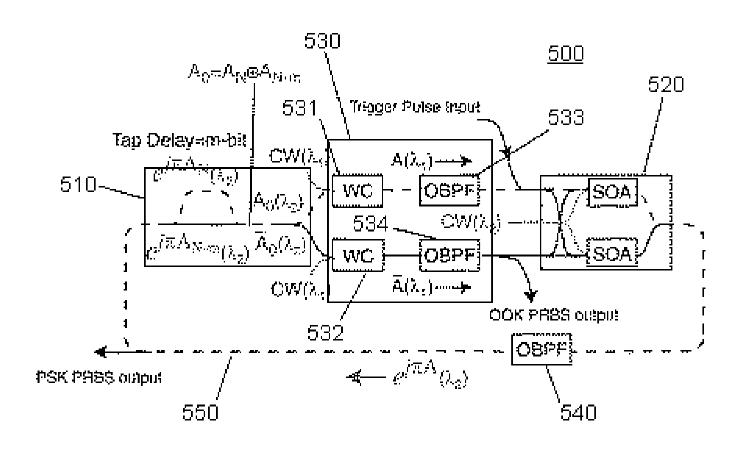
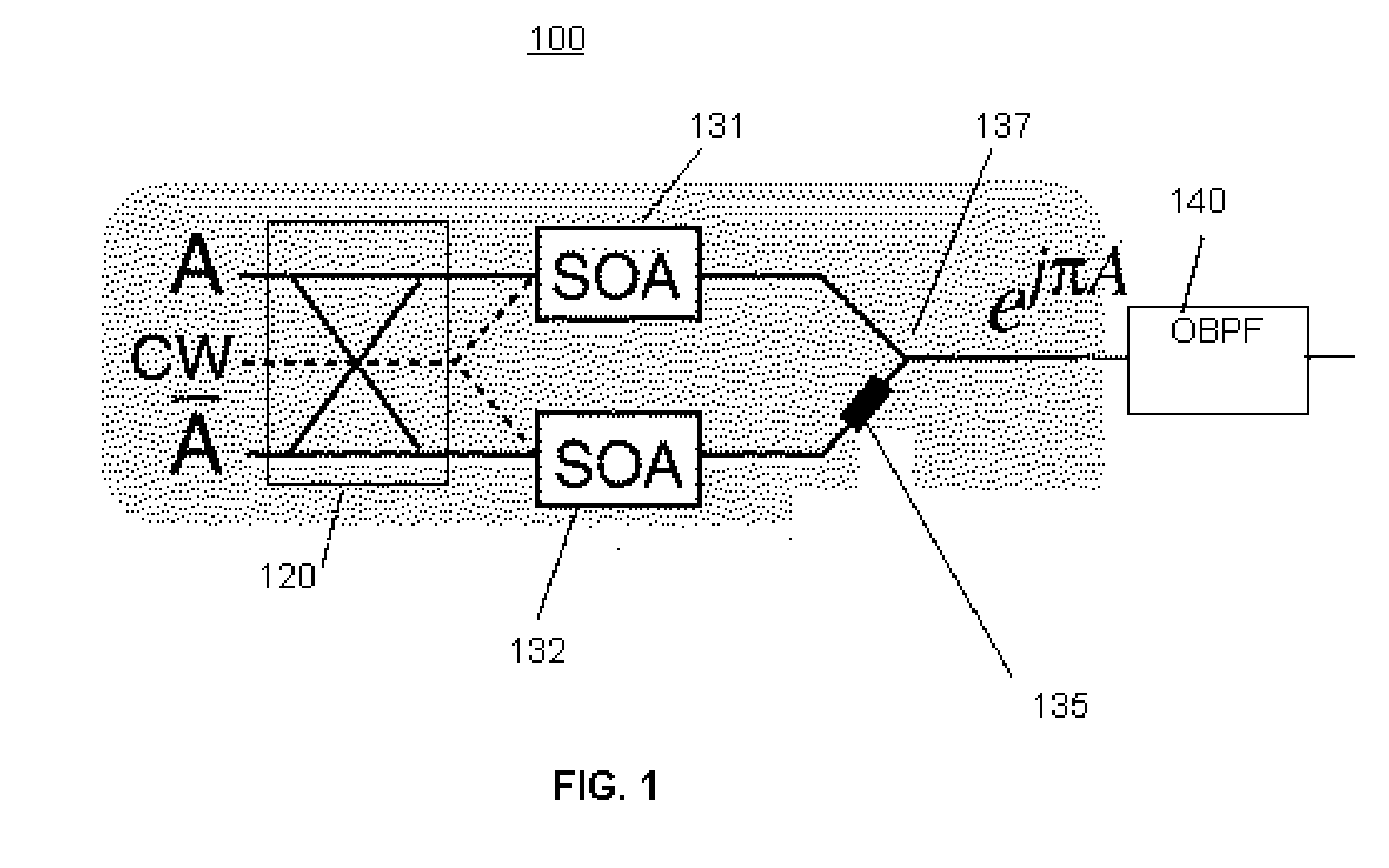
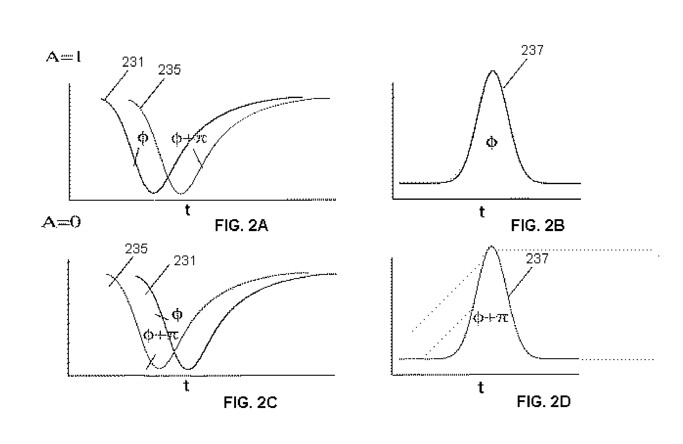
[0017] An exemplary embodiment of an all-optical on-off-keying (OOK) to phase-shift keying (PSK) converter 100 is schematically illustrated in FIG. 1. The converter 100 comprises a differential input stage 120 which is driven by an OOK format signal A and its complement ( A). A first output of the differential input stage 120 is coupled to a first semiconductor optical amplifier (SOA) 131 and a second output of the input stage 120 is coupled to a second SOA 132. The SOAs 131 and 132 are driven with the same continuous wave (CW) laser. The output of the second SOA 132 is coupled to a phase shifter 135 which provides a nominal phase shift of π radians. The output of the phase shifter 135 and the output of the first SOA 131 are combined by a combiner 137 to provide the output of the converter 100.

[0018] In the exemplary embodiment, the SOA-MZI is implemented as a hybrid device fabricated by butt-coupling a bar of InP SOA arrays with input and output silica PLC waveguides. The differen...


PUM


Abstract

An all-optical modulation format converter for converting optical data signals modulated in an on-off-keying (OOK) format to a phase-shift-keying (PSK) format. The OOK-to-PSK converter can be coupled to a delay-line interferometer to provide an all-optical wavelength converter for differential PSK (DPSK). The OOK-to-PSK converter can also be used in all-optical implementations of various functions, including, for example, exclusive-OR (XOR) logic, shift registers, and pseudo-random binary sequence (PRBS) generators.

Description

STATEMENT OF GOVERNMENT INTEREST [0001] The United States Government has certain interests in the present invention.FIELD OF THE INVENTION [0002] The present invention relates to the field of high-speed optical data communications, and in particular, to all-optical methods and systems. BACKGROUND INFORMATION [0003] All-optical signal processing is a key to enabling all-optical networking. All-optical wavelength conversion (AOWC), for example, can be used to perform wavelength routing and contention resolution in transparent optical data networks. As a promising alternative to optical-electrical-optical (OEO) conversion, AOWC can reduce cost and power consumption in high-bit-rate core optical networks. [0004] All-optical format conversion is another functionality needed in all-optical networks composed of multiple modulation formats. For example, all-optical on-off-keying (OOK) to phase-shift-keying (PSK) converters can seamlessly integrate OOK networks and PSK networks. All-optical ...

Claims


Application Information

Patent Timeline
Patent Type & Authority Applications(United States)
IPC IPC(8): H04B10/00H04B10/29
CPCG02F3/00H04B10/5053H04B10/29
Inventor KANG, INUK
Owner WSOU INVESTMENTS LLC
Why Eureka
Try Eureka