Photodiode for multiple wavelength operation

a photodiode and wavelength technology, applied in the field of photodiodes, can solve the problems of substantial loss and/or variation in efficiency, the thickness of respective oxide films forming the ild is not well controlled, and the thickness of respective oxide films is not well controlled

Inactive Publication Date: 2007-03-29
INTERSIL INC
View PDF4 Cites 73 Cited by
  • Summary
  • Abstract
  • Description
  • Claims
  • Application Information

AI Technical Summary

Problems solved by technology

Moreover, the thickness of respective oxide films forming the ILD are not well controlled due to thickness variability predominantly due to ILD layer deposition and pl

Method used


Image

  • Photodiode for multiple wavelength operation
  • Photodiode for multiple wavelength operation
  • Photodiode for multiple wavelength operation

Examples


examples

[0047] It should be understood that the Examples described below are provided for illustrative purposes only and do not in any way define the scope of the invention.

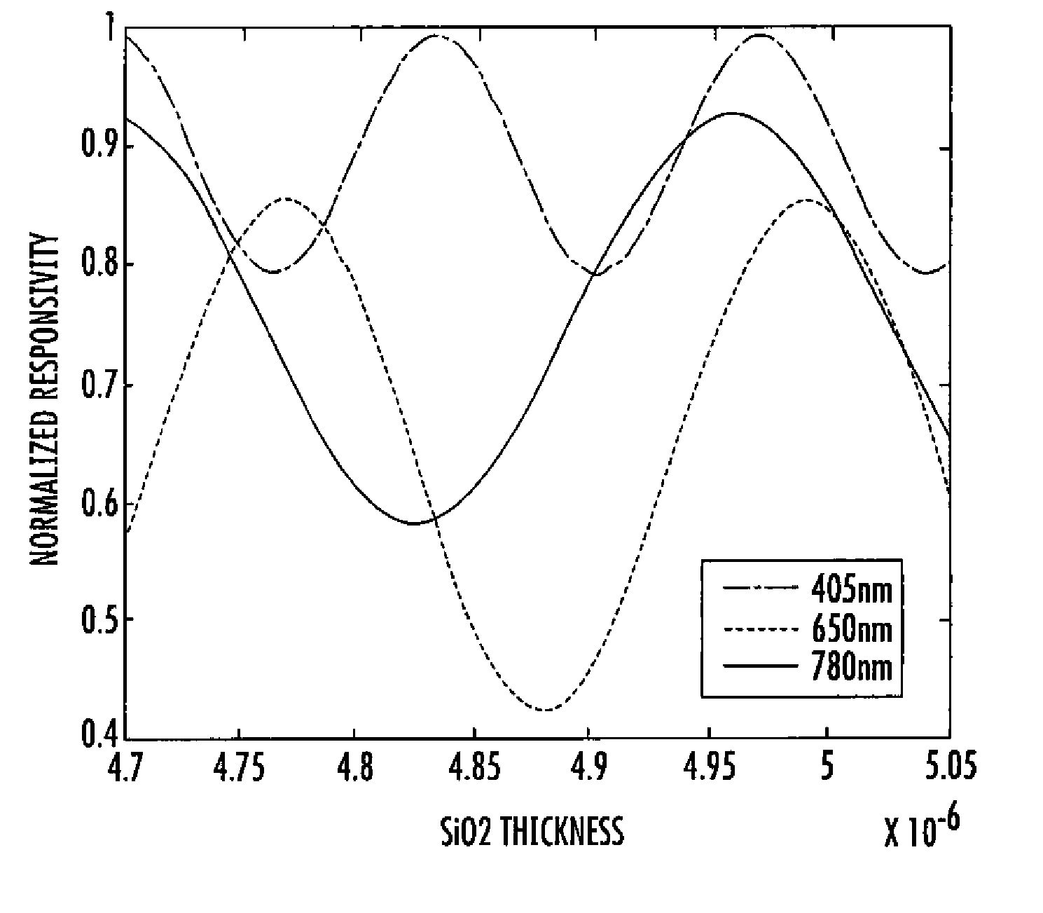
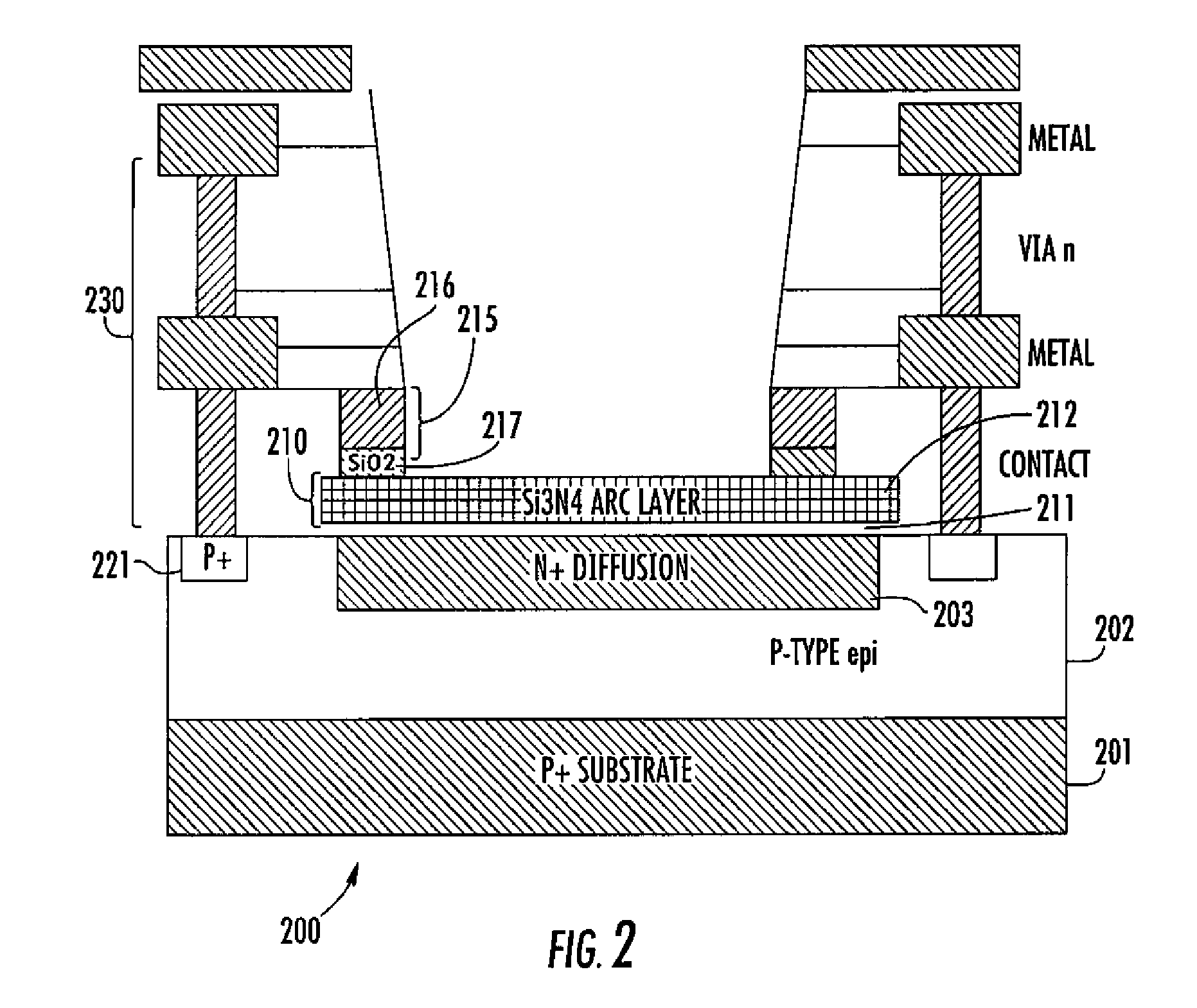
[0048] A simulation was performed to access photodiode response as a function of ARC nitride thickness. The ARC thickness was 3rd order optimized for blue light (405 nm) being about 0.144 um. Overlaying oxide (ILD) and passivation were removed as described above.

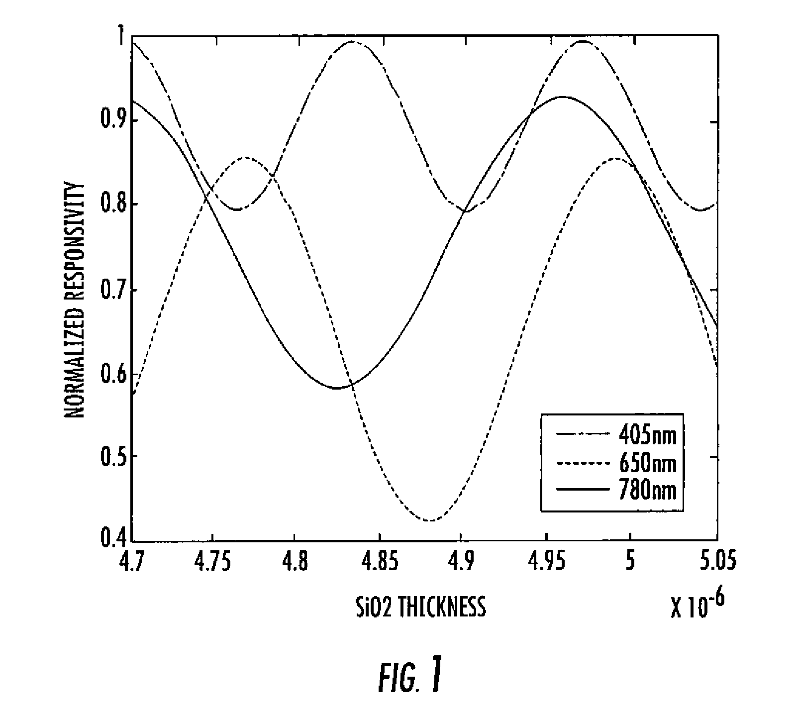
[0049]FIG. 8 shows the normalized response of the PD with the 3rd order ARC (for 405 nm) thickness as a function of the ARC layer thickness (in tens of microns). The rate of change in responsivity can be seen to be low as a function of nitride thickness as compared to the change in responsivity as a function of oxide thickness as shown in FIG. 1. The nitride thickness can be changed to optimize a particular color, or obtain a desired ratio in color responsivitites.


PUM


Abstract

A method of a fabricating a multiple wavelength adapted photodiode and resulting photodiode includes the steps of providing a substrate having a first semiconductor type surface region on at least a portion thereof, implanting and forming a second semiconductor type shallow surface layer into the surface region, and forming a multi-layer anti-reflective coating (ARC) on the shallow surface layer. The forming step includes depositing or forming a thin oxide layer on the shallow surface layer and depositing a second dielectric layer different from the thin oxide layer on the thin oxide layer. An etch stop is formed on the second dielectric, wherein the etch stop includes at least one layer resistant to oxide etch. At least one oxide including layer (e.g. ILD) is then deposited on the etch stop. The oxide including layer and etch stop are then removed to expose at least a portion of the ARC to the ambient.

Description

CROSS-REFERENCE TO RELATED APPLICATIONS [0001] The present application claims priority to Provisional Application No. 60 / 813,910 entitled “PHOTODIODE FOR MULTIPLE WAVELENGTH OPERATION” filed on Jun. 15, 2006; and a continuation-in-part (CIP) of U.S. application Ser. No. 11 / 378,843 entitled “PHOTODIODES WITH ANTI-REFLECTION COATING” filed on Mar. 17, 2006, which claims priority to Provisional Application No. 60 / 663,239 filed on Mar. 18, 2005, all of which are incorporated by reference in their entireties into the present application.FIELD OF THE INVENTION [0002] The invention generally relates to photodiodes, and more particularly to semiconductor photodiodes that have at least one anti-reflective layer, and processes for fabrication to form integrated circuit devices that include photodiodes. BACKGROUND OF THE INVENTION [0003] The structure and function of semiconductor photodiodes are well known. Photodiodes convert photons into electrical energy. Conventional photodiodes operate i...

Claims


Application Information

Patent Timeline
IPC IPC(8): H01L21/00H01L31/113H01L31/0203H01L31/062
CPCH01L27/1462H01L31/02165H01L27/1463
Inventor ZHENG, DONGBENZEL, PHILLIP J.JONES, JOYKALNITSKY, ALEXANDERRATMAN, PERUMAL
Owner INTERSIL INC
Why Eureka
Try Eureka