Semiconductor device and semiconductor device production method

a semiconductor device and semiconductor technology, applied in the direction of semiconductor devices, semiconductor/solid-state device details, printed circuits, etc., can solve the problems of difficult design of semiconductor devices, difficult to provide the planarity required for reliable electrical connections, and increase the possibility of poor connection, so as to reduce the requirement for the connection terminal of semiconductor elements and increase the planarity of the board. , the effect of increasing the planarity

Inactive Publication Date: 2007-04-05
PANASONIC CORP
View PDF1 Cites 8 Cited by
  • Summary
  • Abstract
  • Description
  • Claims
  • Application Information

AI Technical Summary

Benefits of technology

[0038] According to the present invention, the connection electrode is provided in the recess formed in the one major surface of the board, thereby eliminating the need for the provision of the solder resist. Therefore, the warp of the entire board is suppressed which may otherwise occur due to the thermal contraction of the solder resist, thereby increasing the planarity of the board. By increasing the planarity of the board, the planarity requirement for the connection terminal of the semiconductor element is alleviated. Accordingly, the process design flexibility can be increased.
[0039] Further, the deformation of the board is suppressed, so that the warp of the board and the semiconductor element after the mounting of the semiconductor element can be suppressed.
[0040] By increasing the planarity of the board, a load to be applied for correction of the warp and planarization of the board can be reduced. Therefore, a load to be applied when the semiconductor element is mounted on the board can be reduced.
[0041] The reliability of the junctions of the semiconductor element is improved by the effects described above.

Problems solved by technology

This increases the possibility of poorer connection.
However, it is difficult to provide a planarity required for the reliable electrical connection to the connection electrodes because of the warp of the board.
Therefore, it is difficult to design the construction of the semiconductor device to meet demands for an increased number of pins, a reduced pitch and a reduced thickness of the semiconductor element.

Method used


Image

  • Semiconductor device and semiconductor device production method
  • Semiconductor device and semiconductor device production method
  • Semiconductor device and semiconductor device production method

Examples


embodiment 1

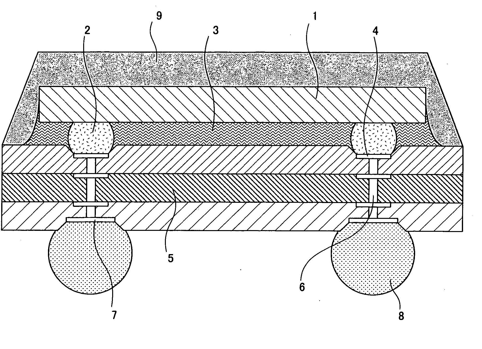
[0051]FIG. 1 is a sectional view illustrating the construction of a semiconductor device according to Embodiment 1 of the present invention. As shown in FIG. 1, no solder resist is provided on front and rear major surfaces of a board 5, and the board 5 includes connection electrodes 4 respectively provided in recesses formed in one major surface thereof, and external electrodes 7 respectively provided in recesses formed in the other major surface thereof. The board 5 further includes vias 6 provided therein and respectively electrically connecting the connection electrodes 4 to the external electrodes 7, and external terminals 8 are respectively provided on the external electrodes 7.

[0052] The depth of the connection electrodes 4 as measured from the one major surface of the board 5 to the surfaces of the connection electrodes 4 and the depth of the external electrodes 7 as measured from the other major surface of the board 5 to the surfaces of the external electrodes 7 are desirab...

embodiment 2

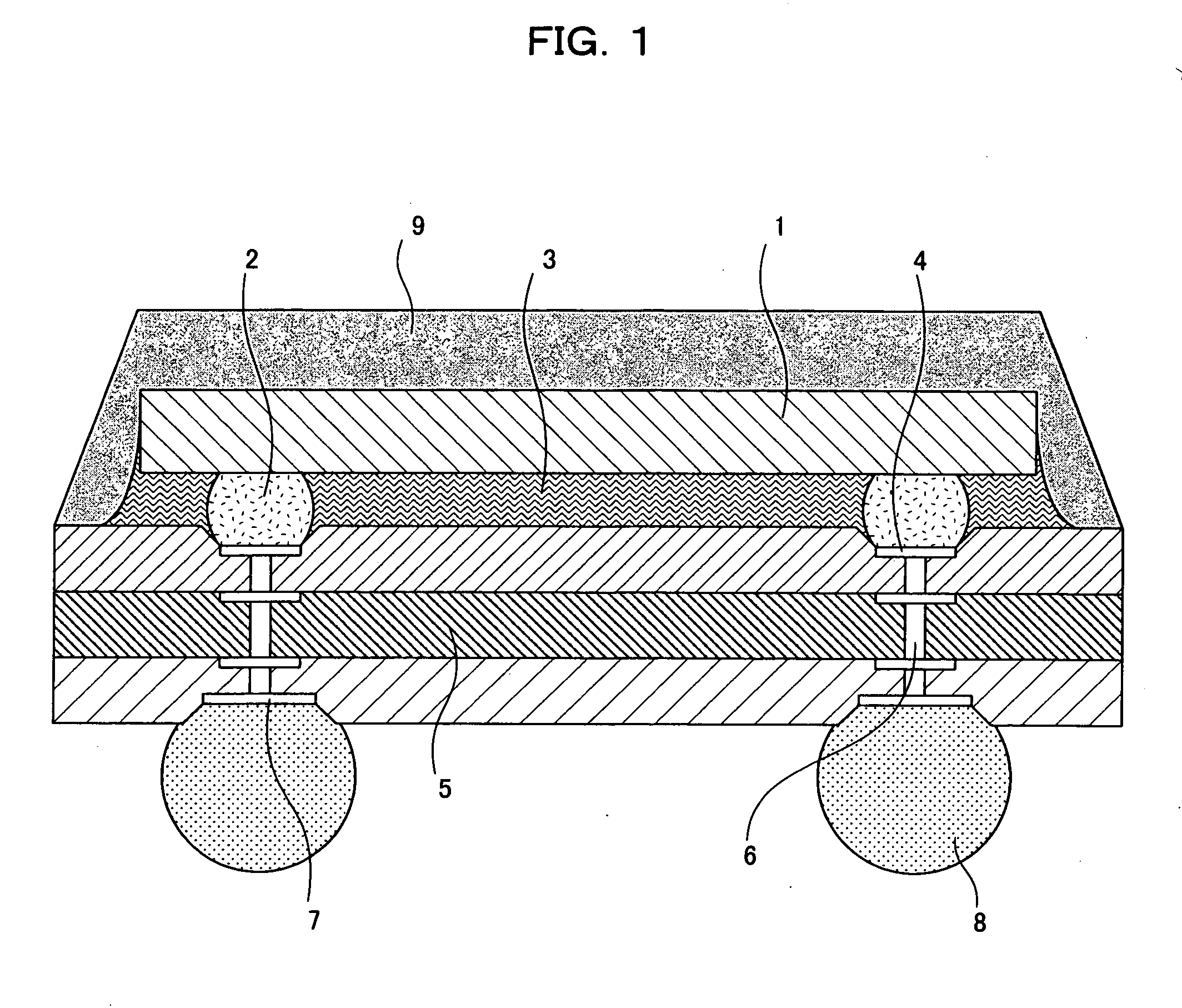
[0066]FIG. 2 is a sectional view illustrating the construction of a semiconductor device according to Embodiment 2 of the present invention. In FIG. 2, connection electrodes 4 are provided in one major surface of a board 5 with their surfaces being flush with the one major surface. External electrodes 7 are respectively provided in recesses formed in the other major surface of the board 5.

[0067] The depth of the external electrodes 7 as measured from the other major surface of the board 5 to the surfaces of the external electrodes 7 is desirably not smaller than 10 μm, which is substantially equal to the thickness of a solder resist layer which would otherwise be provided on the other major surface. The other arrangement of Embodiment 2 is the same as in Embodiment 1, and will not be described in detail.

[0068] With this arrangement, the external electrodes 7 are respectively provided in the recesses formed in the other major surface of the board 5. Therefore, where the external te...

embodiment 3

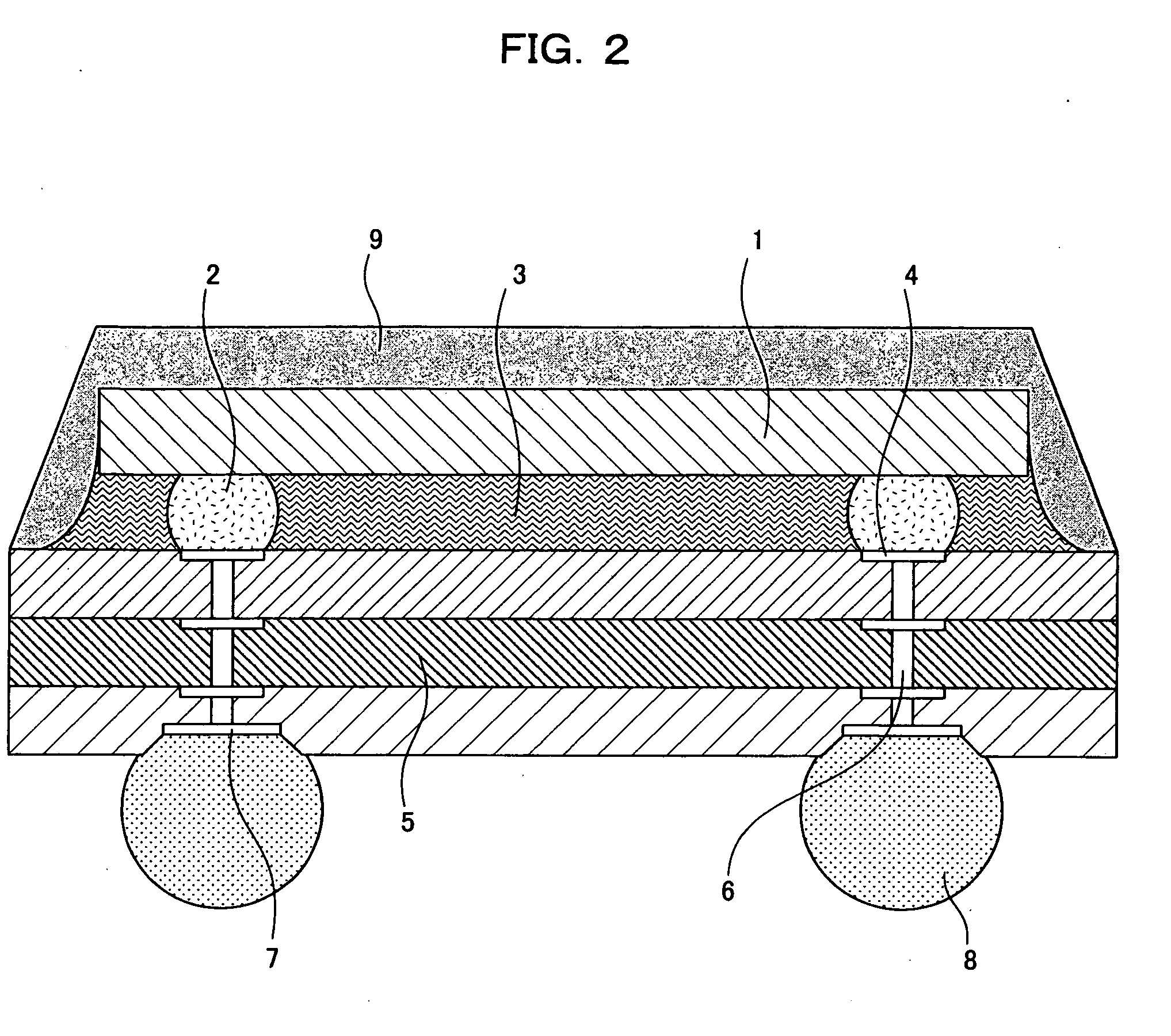
[0071]FIG. 3 is a sectional view illustrating the construction of a semiconductor device according to Embodiment 3 of the present invention. In FIG. 3, connection electrodes 4 are respectively provided in recesses formed in one major surface of a board 5. The depth of the connection electrodes 4 as measured from the one major surface of the board 5 to the surfaces of the connection electrodes 4 is desirably not smaller than 10 μm, which is substantially equal to the thickness of a solder resist layer which would otherwise be provided on the one major surface.

[0072] External electrodes 7 are provided in the other major surface of the board 5 as being exposed from openings formed in a solder resist 10 formed on the other major surface of the board 5. The surfaces of the external electrodes 7 are flush with the other major surface of the board 5. The other arrangement of Embodiment 3 is the same as in Embodiment 1, and will not be described in detail.

[0073] In the semiconductor devic...


PUM


Abstract

The present invention provides a semiconductor device in which the warp of a board is suppressed without the need for provision of a solder resist on opposite surfaces of the board and semiconductor element connection characteristics are improved by reducing stress exerted on a connection portion, and increases flexibility in assembly process.

Description

FIELD OF THE INVENTION [0001] The present invention relates to a semiconductor device and a semiconductor device production method. More specifically, the present invention relates to a semiconductor device which ensures protection of an integrated circuit portion of an LSI chip, stable electrical connection between the LSI chip and an external device and higher density mounting and, particularly, relates to a semiconductor device including a semiconductor element having a multiplicity of connection terminals. BACKGROUND OF THE INVENTION [0002] With recent trend toward size and weight reduction in the fields of information communication devices, office electronic devices, domestic electronic devices, measurement devices, industrial electronic devices such as assembly robots, medical electronic devices and electronic toys, there has been a heavy demand for reduction of the packaging area of semiconductor devices. [0003] To meet the demand, BGA (ball grid array) packages and the like ...

Claims


Application Information

Patent Timeline
Patent Type & Authority Applications(United States)
IPC IPC(8): H01L23/12
CPCH01L23/49816H01L2224/16225H01L2224/13144H01L2224/13147H01L2224/16237H01L2224/81203H01L2224/81801H01L2224/83102H01L2224/83192H01L2224/92125H01L2924/01029H01L2924/01033H01L2924/01078H01L2924/01079H01L2924/01082H01L2924/14H01L2924/15311H01L2924/3511H05K1/113H05K2201/09472H05K2201/096H05K2201/10674H01L2924/01006H01L2924/01047H01L2924/0105H01L2924/014H01L2224/16235H01L2224/81024H01L2224/73204H01L2224/32225H01L24/81H01L2924/00H01L2924/181
Inventor OSUMI, TAKATOSHI
Owner PANASONIC CORP
Why Eureka
Try Eureka