
Method and computer program for incremental placement and routing with nested shells

Inactive Publication Date: 2007-04-05
BELL SEMICON LLC
View PDF3 Cites 12 Cited by
  • Summary
  • Abstract
  • Description
  • Claims
  • Application Information

AI Technical Summary

Problems solved by technology

For example, if the propagation delay is too long in a path that propagates a clock signal to a flip-flop, the flip-flop may not be set to the correct value when the clock signal arrives, resulting in a timing violation.
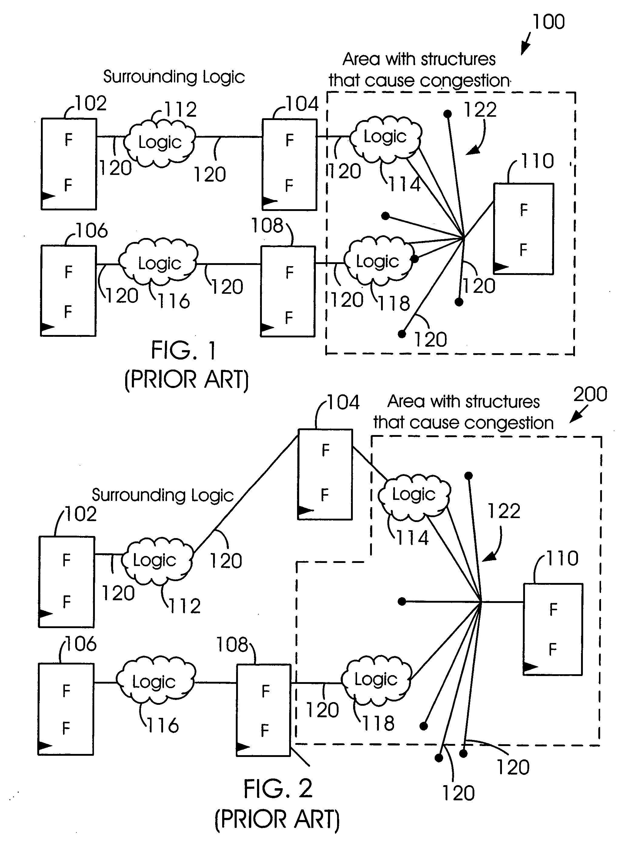
Also, signal routing congestion may occur in locations where there are more signals to route than there is available routing area on the chip.
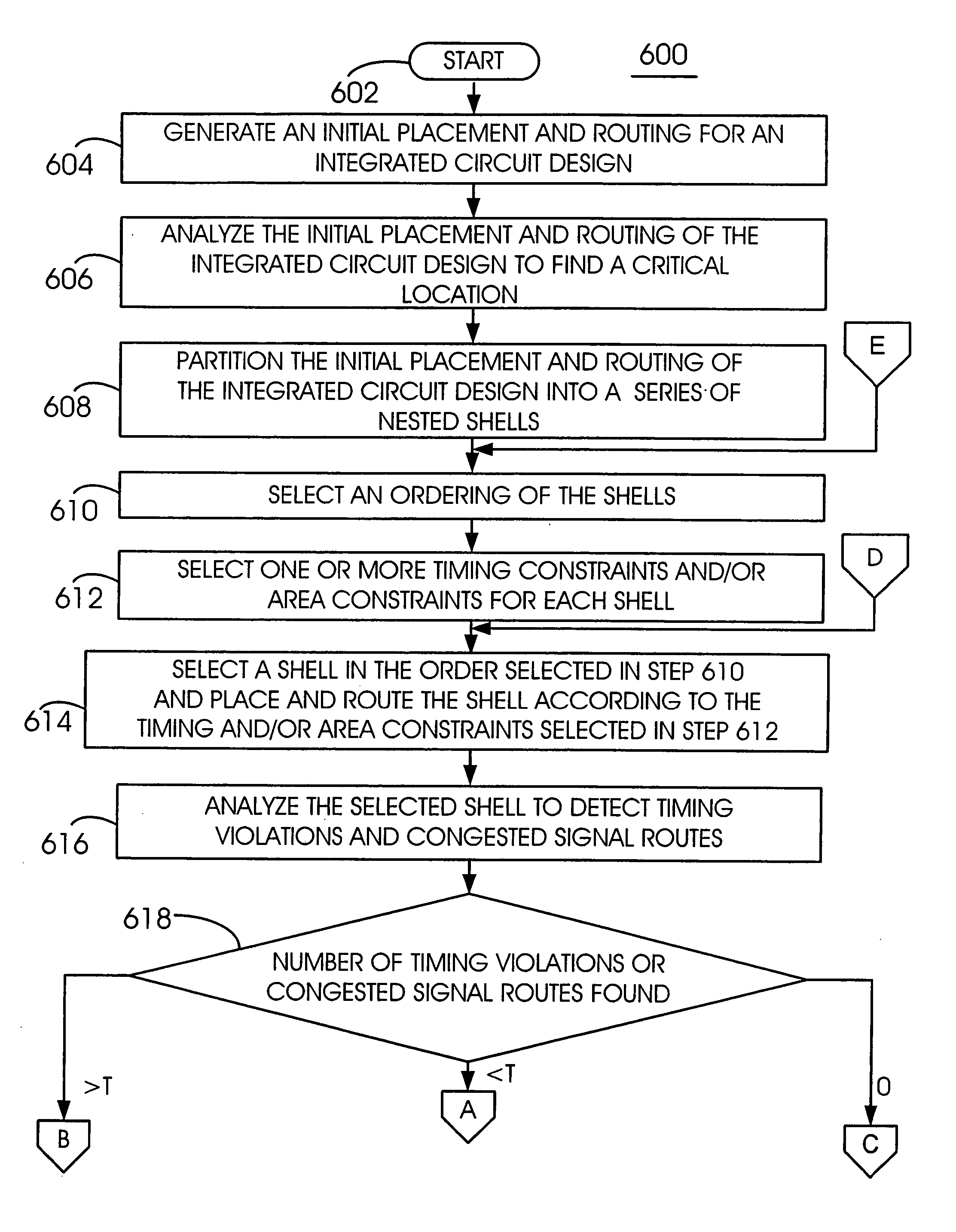
Timing closure is a resource-intensive task in which all timing violations and congested signal routes in the placement and routing must be resolved before an integrated circuit design may be taped out, that is, generated in mask form for depositing and etching layers of various materials on a silicon substrate.

Method used


Image

  • Method and computer program for incremental placement and routing with nested shells
  • Method and computer program for incremental placement and routing with nested shells
  • Method and computer program for incremental placement and routing with nested shells

Examples


Embodiment Construction

[0024] The following description is not to be taken in a limiting sense, rather for the purpose of describing by specific examples the general principles that are incorporated into the illustrated embodiments. For example, certain actions or steps may be described or depicted in a specific order to be performed. However, practitioners of the art will understand that the specific order is only given by way of example and that the specific order does not exclude performing the described steps in another order to achieve substantially the same result. Also, the terms and expressions used in the description have the ordinary meanings accorded to such terms and expressions in the corresponding respective areas of inquiry and study except where other meanings have been specifically set forth herein.

[0025]FIG. 1 illustrates a typical placement and routing diagram 100 for an integrated circuit design of the prior art. Shown in FIG. 1 are flip-flops 102, 104, 106, 108, and 110, logic clouds...


PUM


Abstract

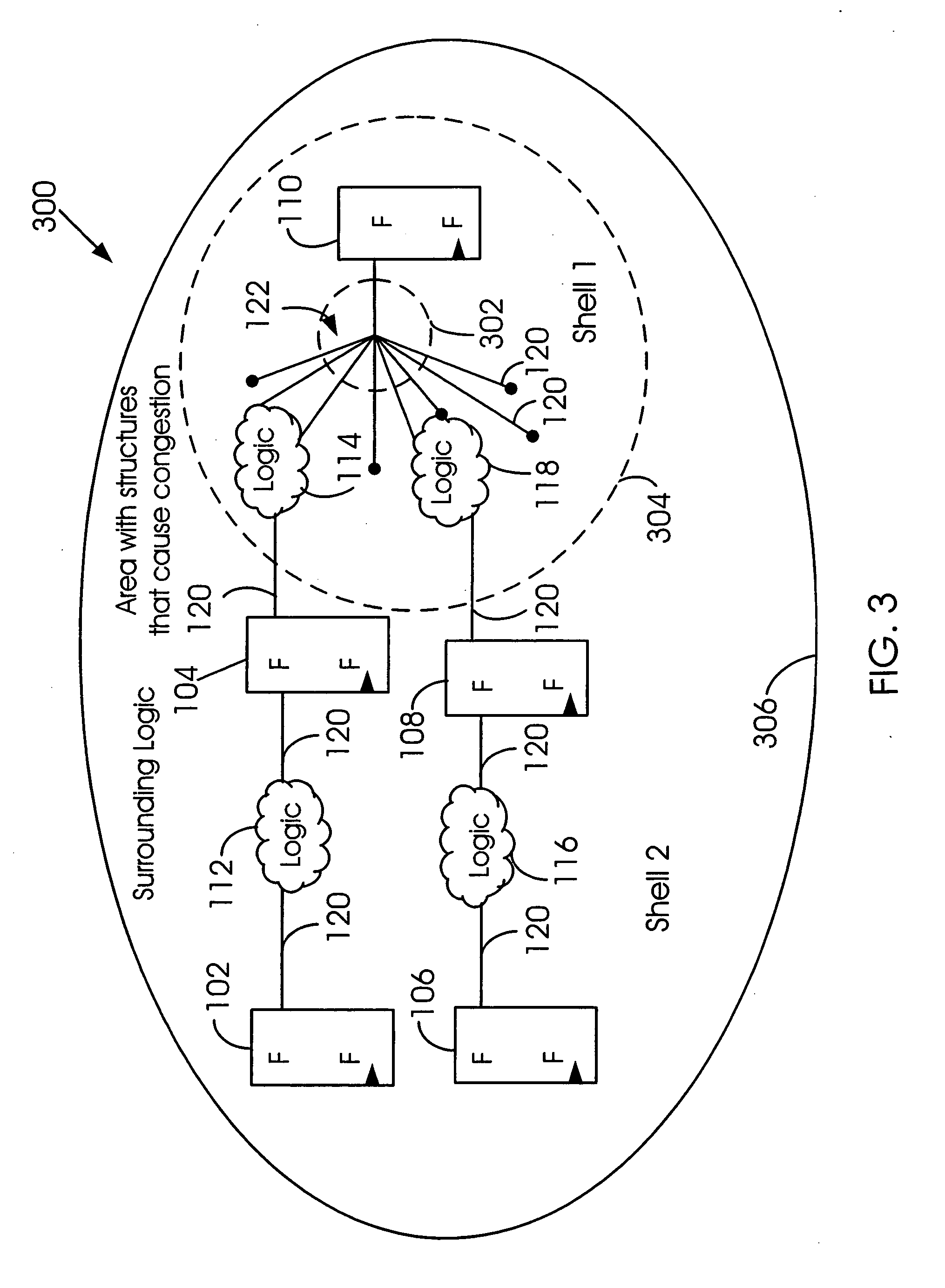
A method of placing and routing an integrated circuit design includes steps of (a) generating an initial placement and routing for at least a portion of an integrated circuit design; (b) analyzing the initial placement and routing of the integrated circuit design to find a critical location; (c) partitioning the initial placement and routing of the integrated circuit design into a series of nested shells wherein each shell surrounds the critical location and each preceding shell; (d) selecting an ordering of the shells; (e) selecting at least one of a timing constraint and an area constraint for each shell; and (f) placing and routing each shell in the order selected in step (d) according to the at least one timing constraint and area constraint selected in step (e).

Description

BACKGROUND OF THE INVENTION [0001] 1. Field of the Invention [0002] The present invention is directed to the design and manufacture of integrated circuits. More specifically, but without limitation thereto, the present invention is directed to methods of placement and routing for an integrated circuit design. [0003] 2. Description of Related Art [0004] An important phase in the design of an integrated circuit is to verify that each logic path in the integrated circuit design meets all timing constraints required to meet performance specifications. The verification of the timing for each logic path in an integrated circuit design is typically called timing closure. For example, if the propagation delay is too long in a path that propagates a clock signal to a flip-flop, the flip-flop may not be set to the correct value when the clock signal arrives, resulting in a timing violation. Also, signal routing congestion may occur in locations where there are more signals to route than there...

Claims


Application Information

Patent Timeline
IPC IPC(8): G06F17/50
CPCG06F17/5072G06F17/5077G06F30/392G06F30/394
Inventor LAHNER, JUERGEN K.BALASUBRAMANIAN, BALAMURUGANFRY, RANDALL P.
Owner BELL SEMICON LLC
Learn More