Method of etching carbon-containing layer and method of fabricating semiconductor device

a technology of etching carbon and etching carbon, which is applied in the direction of semiconductor/solid-state device manufacturing, basic electric elements, electric devices, etc., can solve the problems of difficult to obtain the desired etch selectivity of acl relative to the etching layer, the thickness of the photoresist layer is decreased, and the difficulty of putting protective carbon series polymer on the capping layer, etc., to achieve the effect of high aspect ratio

Active Publication Date: 2007-04-12
SAMSUNG ELECTRONICS CO LTD
View PDF7 Cites 13 Cited by
  • Summary
  • Abstract
  • Description
  • Claims
  • Application Information

AI Technical Summary

Benefits of technology

[0013] The present invention also provides a method of fabricating a semiconductor device in which a contact hole is formed using an etch mask for etching the carbon-containing layer having sufficient etch resistance to achieve the desired results. In the method, when forming a contact hole having a high aspect ratio as needed to form a contact for a highly integrated semiconductor device, neighboring contact holes maintain a small but distinct distance from each other upon etching even when an interval between neighboring contact holes is as narrow as several tens of nm or less, thereby preventing short-circuits between neighboring contacts.
[0019] According to a particular embodiment of the present invention, plasma of a carbon-etching mixture gas including O2 and a Si-containing gas is used to anisotropically etch a carbon-containing layer which is, in turn, intended to be used as a second etch mask, such that a Si series polymer residue layer (which is an etching residue) is formed on the capping layer pattern that is being used as the first etching mask during the step of etching the carbon-containing layer. Accordingly, the capping layer pattern is protected by the Si polymer residue such that a sufficient etch selectivity of the capping layer pattern relative to the carbon-containing layer is obtained. In addition, it is possible to perform etching so that a hole obtained by etching the carbon-containing layer has a smaller CD at a bottom portion thereof than at a top portion thereof, which is an inlet of the hole. Accordingly, the present invention is particularly advantageous when applied to the formation of a contact hole having a high aspect ratio as needed to form a contact for a highly integrated semiconductor device.

Problems solved by technology

Therefore, the thickness of the photoresist layer is decreased, and a relatively thin photoresist layer leads to a number of problems.
Thus, when etching the ACL using an etching gas that also includes the fluorocarbon series gas, it is difficult to deposit the protective carbon series polymer on the capping layer, and, accordingly, a desired etch selectivity of the ACL relative to the capping layer is difficult to obtain.
However, it is difficult to etch the pattern with the inclined sidewall profile following such polymer deposition.

Method used


Image

  • Method of etching carbon-containing layer and method of fabricating semiconductor device
  • Method of etching carbon-containing layer and method of fabricating semiconductor device
  • Method of etching carbon-containing layer and method of fabricating semiconductor device

Examples


Embodiment Construction

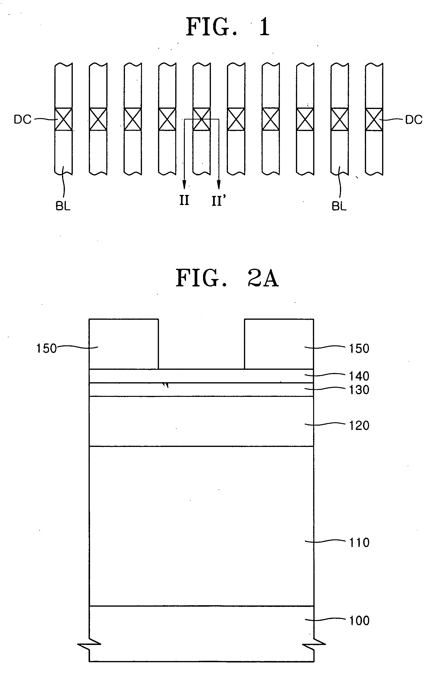
[0026]FIG. 1 schematically illustrates the layout of a primary portion of an exemplary semiconductor device wherein a method of fabricating a semiconductor device according to an embodiment of the present invention is advantageously applicable.

[0027] More particularly, the layout of a portion of a cell block constituting a NAND type flash memory device is illustrated in FIG. 1. Particularly, the layout of direct contacts DC connected to bit lines BL is illustrated. In a recent design rule, the direct contacts DC are arranged at intervals of several tens of nm, for example, about 20 to 40 nm. The present invention provides effective and efficient methods of forming patterns that are arranged at such relatively narrow intervals as described above using an amorphous carbon layer (ACL) pattern as an etch mask.

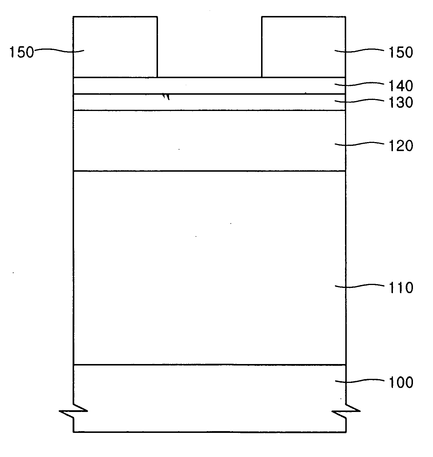
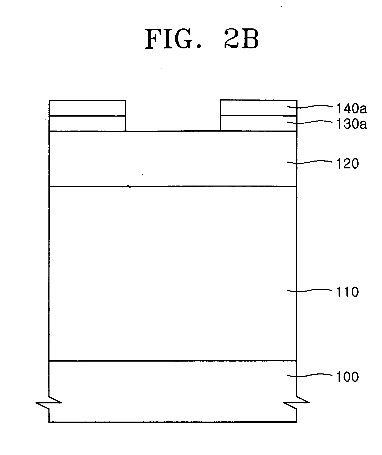
[0028]FIGS. 2A through 2D are schematic cross-sectional views illustrating a method of fabricating a semiconductor device according to an embodiment of the present invention. FIG...


PUM

PropertyMeasurementUnit
temperatureaaaaaaaaaa
widthaaaaaaaaaa
total volumeaaaaaaaaaa

Abstract

A method of etching a carbon-containing layer on a semiconductor substrate using a Si-containing gas and a related method of fabricating a semiconductor device in which a plurality of contact holes having excellent sidewall profiles are formed by etching an interlayer insulating layer using a carbon-containing layer pattern formed in accordance with the invention and having a width of several tens of nm as an etch mask are provided. To etch a carbon-containing layer to be used as a second etch mask, a first mask pattern is formed on the carbon-containing layer to partially expose a top surface of the carbon-containing layer. The carbon-containing layer is then anisotropically etched with a plasma of a carbon-etching mixture gas formed of O2 and a Si-containing gas using the first mask pattern as a first etch mask to form the carbon-containing layer pattern. Neighboring contact holes in a high-density cell array region fabricated in accordance with this invention are distinctly separated from each other, even when an interval between the neighboring contact holes is as small as several tens of nm or less; and, thus, a short-circuit between neighboring unit cells using such contact holes can be prevented.

Description

CROSS-REFERENCE TO RELATED PATENT APPLICATION [0001] This application claims the benefit of Korean Patent Application No. 10-2005-0096164, filed on Oct. 12, 2005, in the Korean Intellectual Property Office, the disclosure of which is incorporated herein in its entirety by reference. BACKGROUND OF THE INVENTION [0002] 1. Field of the Invention [0003] The present invention relates to an etching method for use in connection with semiconductor device fabrication and to a method of fabricating a semiconductor device using the same, and more particularly, to a method of etching a carbon-containing layer using a new etching gas and to a method of fabricating a semiconductor device using the same. [0004] 2. Description of the Related Art [0005] As semiconductor devices have become more integrated and the feature size thereof has correspondingly decreased, the horizontal areas of the semiconductor devices have also decreased while the thicknesses of such semiconductor devices have increased....

Claims


Application Information

Patent Timeline
Patent Type & Authority Applications(United States)
IPC IPC(8): H01L21/465
CPCH01L21/02063H01L21/31116H01L21/0214H01L21/3065H01L21/02362
Inventor BAI, KEUN-HEE
Owner SAMSUNG ELECTRONICS CO LTD
Why Eureka
Try Eureka