Micromechanical component having an anodically bonded cap and a manufacturing method

a micromechanical and cap technology, applied in the field of micromechanical components, can solve the problems of high cost, high manufacturing cost, and electrical access produced from the back side of the sensor substrate with some degree of technological complexity, and achieve the effects of reducing the surface area of the sensor chip, cost-effective, and keeping the technological expenditure small

Inactive Publication Date: 2007-04-19
ROBERT BOSCH GMBH
View PDF11 Cites 6 Cited by
  • Summary
  • Abstract
  • Description
  • Claims
  • Application Information

AI Technical Summary

Benefits of technology

[0017] In this context, a method for structuring an anodically bondable composite cap wafer is advantageously described, which permits electrical contacting of the sensor structures located below the cap wafer. The method described allows a significant reduction in the surface of the sensor chip compared to the existing sealing-glass encapsulation techniques, and keeps the technological expenditure small, especially compared to methods which include backside contacting. Therefore, it represents a comparatively cost-effective alternative for encapsulating inertial sensors and other micromechanical sensors by anodic bonding methods. The possible cost advantage compared to a backside contacting lies in the avoidance or the replacement of several ...

Problems solved by technology

Because the composite cap is difficult to structure, when working with MPT, for example, the electrical accesses are produced from the back side of the sensor substrate with some degree of technological complexity.
Moreover, the complicated backside contacting requires planarization of t...

Method used


Image

  • Micromechanical component having an anodically bonded cap and a manufacturing method
  • Micromechanical component having an anodically bonded cap and a manufacturing method
  • Micromechanical component having an anodically bonded cap and a manufacturing method

Examples


Embodiment Construction

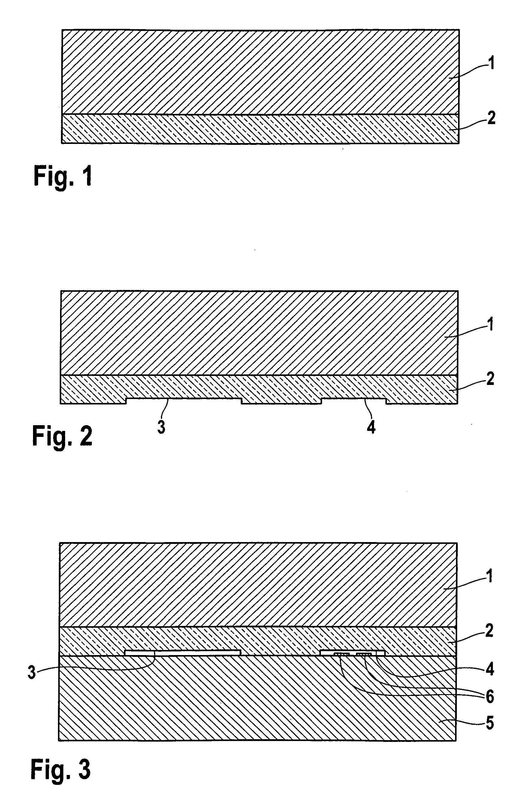
[0029]FIG. 1 shows a cap wafer in the form of a composite cap wafer made up of a first silicon substrate 1 and a thin glass substrate 2. Thin glass substrate 2 is intended to permit the anodic bondability of the cap wafer.

[0030]FIG. 2 shows a first recess 4 and a further recess 3 which are introduced into thin glass substrate 2 of the cap wafer.

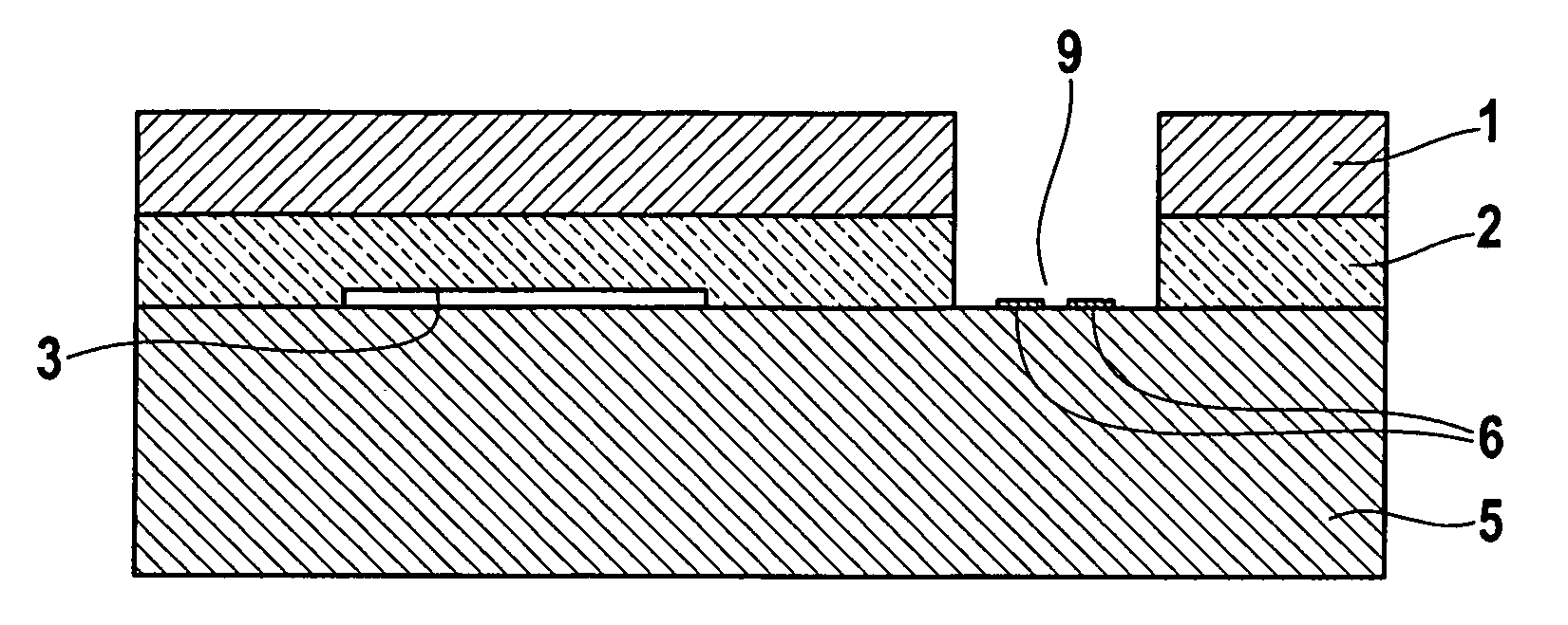
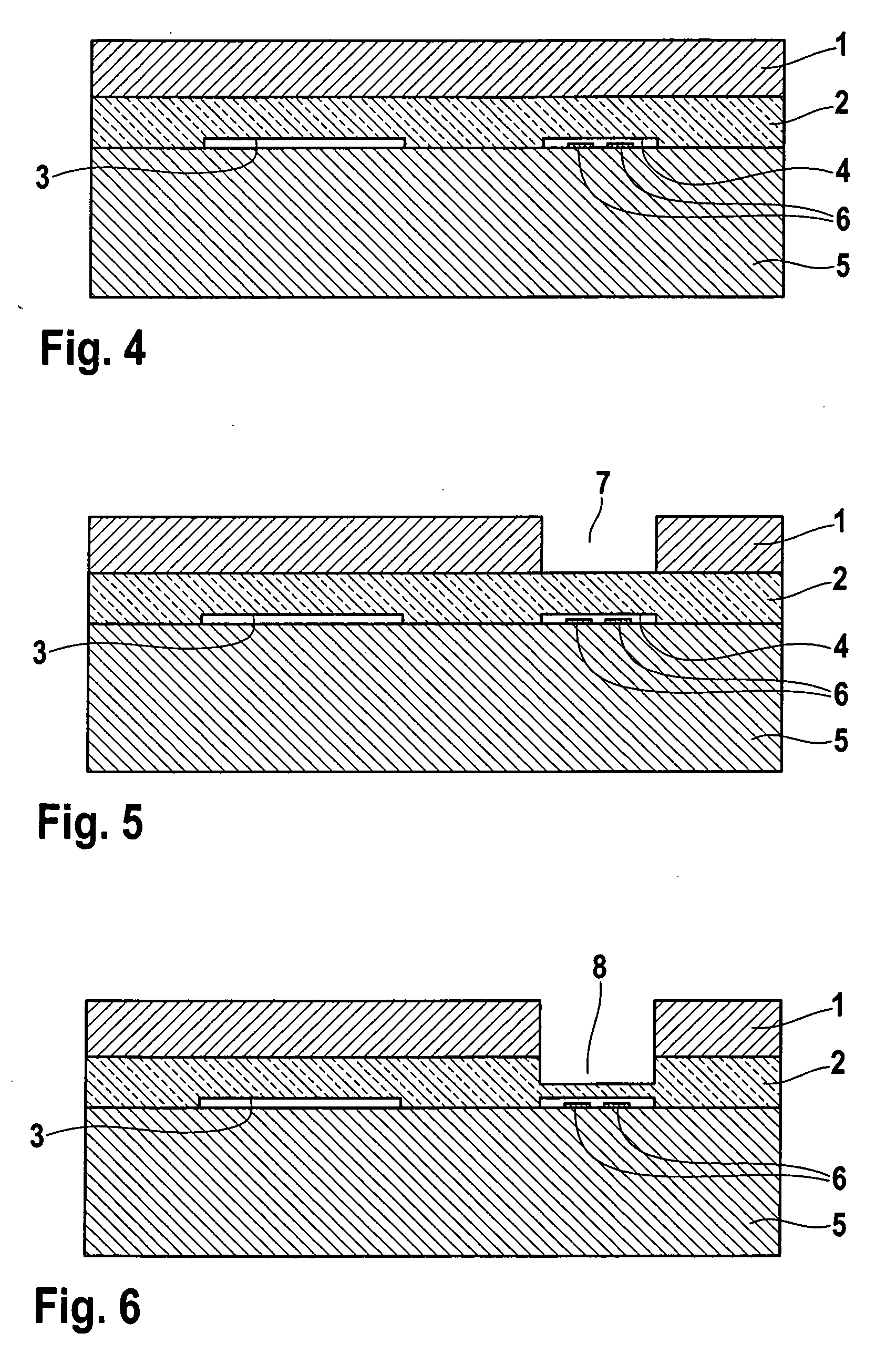
[0031]FIG. 3 shows the anodic bonding of the composite cap wafer, made up of first silicon substrate 1 and thin glass substrate 2, to a functional wafer. The functional wafer is made up of at least a second silicon substrate 5 and has at least one electrical contact surface 6 as well as, on the same side, a micromechanical structure which is not shown separately. After the bonding, first recess 4 forms a cavity over electrical contact surface 6. Further recess 3 forms a cavity over the micromechanical structure and protects this structure by encapsulation.

[0032]FIG. 4 shows the thinning of first silicon substrate 1 of the cap wafer on the ...


PUM


Abstract

A micromechanical component includes a cap wafer made up of at least a first silicon substrate and a thin glass substrate, and having a functional wafer made up of at least a second silicon substrate, at least one electrical contact surface being disposed on the functional wafer. The cap wafer is joined at the glass substrate to the functional wafer by anodic bonding. The electrical contact surface is disposed on a side of the functional wafer facing the cap wafer, and the cap wafer has at least one recess, such that an access is provided to the electrical contact surface. A method for encapsulating a micromechanical component having a cap wafer, by anodically bonding the cap wafer to a functional wafer.

Description

FIELD OF THE INVENTION [0001] The present invention relates to a micromechanical component having a cap wafer made up of at least a first silicon substrate and a thin glass substrate, and having a functional wafer made up of at least a second silicon substrate, at least one electrical contact surface being disposed on the functional wafer. The cap wafer is joined at the glass substrate to the functional wafer by anodic bonding. The present invention further relates to a method for encapsulating (packaging) a micromechanical component having a cap wafer, by anodically bonding the cap wafer to a functional wafer. The present invention further relates to a method for structuring the composite cap that is compatible with the electrical contacting in the sealing-glass encapsulation technology customary under the state of the art, and using which, it is possible to dispense with the technologically costly backside contacting. BACKGROUND INFORMATION [0002] Inertial sensors are usually enca...

Claims


Application Information

Patent Timeline
IPC IPC(8): H01L21/00H01L29/76H01L29/94H01L31/00B81C99/00
CPCB81B2207/095B81C2203/0109B81C1/00301
Inventor STAHL, HEIKOULBRICH, NICOLAUSSTRAUB, RAINER
Owner ROBERT BOSCH GMBH
Why Eureka
Try Eureka