Organic thin film transistor and flat panel display device having the same

Inactive Publication Date: 2007-04-26
SAMSUNG DISPLAY CO LTD
View PDF10 Cites 13 Cited by
  • Summary
  • Abstract
  • Description
  • Claims
  • Application Information

AI Technical Summary

Benefits of technology

[0010] Aspects of the present invention provide an organic thin film transistor that can control threshold vo

Problems solved by technology

However, due to high contact resistance between the metal and the semiconductor layer, device characteristics are reduced, thereby increasing

Method used


Image

  • Organic thin film transistor and flat panel display device having the same
  • Organic thin film transistor and flat panel display device having the same
  • Organic thin film transistor and flat panel display device having the same

Examples


Embodiment Construction

[0028] Reference will now be made in detail to the present embodiments of the present invention, examples of which are illustrated in the accompanying drawings, wherein like reference numerals refer to the like elements throughout. The embodiments are described below in order to explain the present invention by referring to the figures.

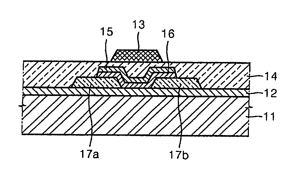
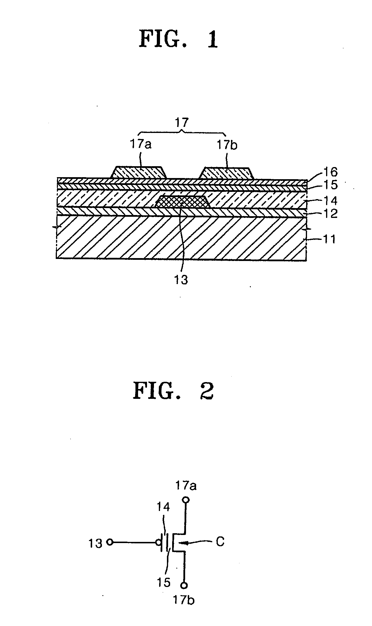
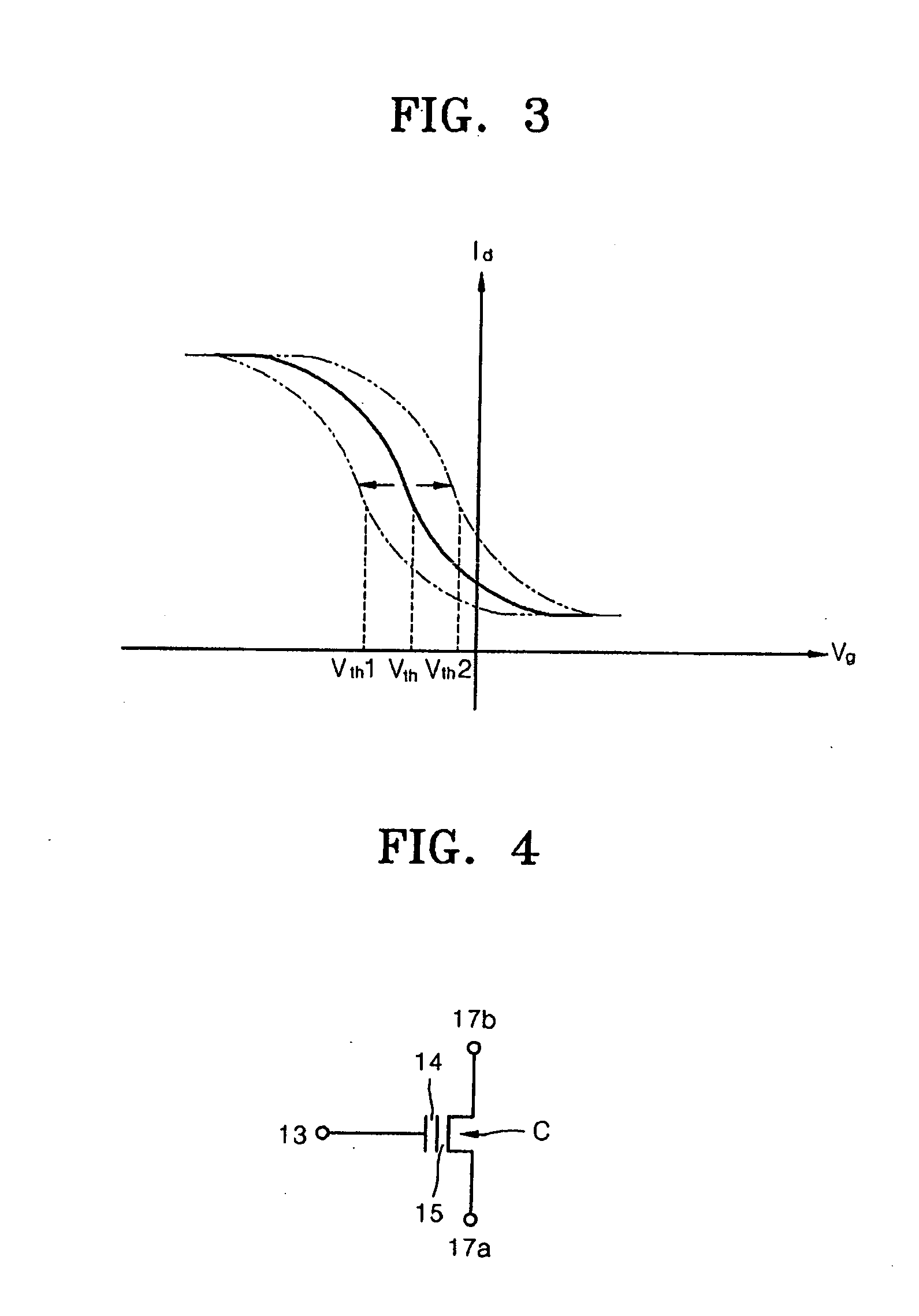
[0029]FIG. 1 is a cross-sectional view of an organic thin film transistor according to an embodiment of the present invention.

[0030] Referring to FIG. 1, the organic thin film transistor is formed on a substrate 11.

[0031] The substrate 11 can be formed of a plastic material such as acryl, polyimide, polycarbonate, polyester, mylar, etc., but is not limited thereto. The substrate 11 can also be formed of a metal such as stainless steel (SUS), tungsten, etc. and glass, and may be flexible.

[0032] An insulating layer 12 such as a barrier layer and / or a buffer layer can be formed on an upper surface of the substrate 11 to prevent the diffusion of impur...


PUM


Abstract

An organic thin film transistor that can control the threshold voltage and reduce leakage current includes: a gate electrode; an organic semiconductor layer insulated from the gate electrode; a source electrode and a drain electrode insulated from the gate electrode and electrically connected to the organic semiconductor layer; a gate insulating layer interposed between the gate electrode and the organic semiconductor layer; and a hole control layer that is interposed between the gate insulating layer and the organic semiconductor layer. The hole control layer includes a compound having a hole-donor group or a compound having a hole-acceptor group.

Description

CROSS-REFERENCE TO RELATED APPLICATIONS [0001] This application claims the benefit of Korean Patent Application No. 2005-99943, filed on Oct. 22, 2005, in the Korean Intellectual Property Office, the disclosure of which is incorporated herein in its entirety by reference. BACKGROUND OF THE INVENTION [0002] 1. Field of the Invention [0003] Aspects of the present invention relate to an organic thin film transistor and a flat panel display device having the organic thin film transistor, and more particularly, to an organic thin film transistor that can shift a threshold voltage to a desired direction, and a flat panel display device having the organic thin film transistor. [0004] 2. Description of the Related Art [0005] Thin film transistors (TFTs) used for flat panel display devices such as a liquid crystal display devices, organic light emitting display devices, or inorganic light emitting display device are used as switching devices that control the operation of each pixel and drivi...

Claims


Application Information

Patent Timeline
IPC IPC(8): H01L29/08H01L29/76H01L35/24H01L29/10H01L51/00H01L31/036H01L31/112
CPCH01L51/0545H01L51/0558H10K10/466H10K10/484H10K10/474
Inventor PARK, JIN-SEONGSUH, MIN-CHULAHN, TAEK
Owner SAMSUNG DISPLAY CO LTD
Why Eureka
Try Eureka