Semiconductor memory

Active Publication Date: 2007-04-26
SOCIONEXT INC
View PDF12 Cites 37 Cited by
  • Summary
  • Abstract
  • Description
  • Claims
  • Application Information

AI Technical Summary

Benefits of technology

[0012] In a preferable example of the first aspect of the invention, the precharge voltage generating circuit outputs a first precharge voltage when the ambient temperature is equal to or lower than a boundary temperature, and it outputs a second precharge voltage when the ambient temperature is higher than the boundary temperature. That is, the precharge voltage generating circuit outputs either of the two kinds of precharge voltages in accordance with the ambient temperature. Minimizing the number of the kinds of the precharge voltages switched in accordance with the ambient temperature can facilitate a switching control, and prevent a circuit scale from enlarging.
[0013] In a preferable example of the first aspect of the invention, the sense amplifier changes a voltage of the bit line to a power supply voltage VII or a ground voltage by the amplifying operation. The first and second precharge voltages which the precharge voltage generating circuit outputs are VII/2 and a voltage lower than VII/2, respectively. As stated above, the data retaining time of the memory cell retaining the “1 data” decreases as the ambient temperature increases. Lowering the precharge voltage at the high temperature and increasing the read margin of the “1 data” makes it possible to increase the worst value of the data retaining time. As a result, the frequency of refreshes lowers, so that the standby current can be reduced.
[0014] In a preferable example of the first aspect of the invention, the sense amplifier changes the voltage of the bit line to a power supply voltage VII or a ground voltage by the amplifying operation. The first and second precharge voltages which the precharge voltage generating circuit outputs are a voltage higher than VII/2 and VII/2, respectively. That is, the precharge voltage heightens at the low temperature, the read margin of the “1 data” decreases, and the read margin of “1 data” increases. The read margin of the “1 data” at the low temperature, which is originally sufficiently long, is decreased, and the decrease is allocated to the read margin of the “0 data”, whereby the data retaining time (worst value) at the low temperature can be lengthened. As a result, the frequency of refreshes lowers, so that the standby current

Problems solved by technology

Therefore, in the case where the DRAM is used as the work memory of the portable terminal, electric power is con

Method used


Image

  • Semiconductor memory
  • Semiconductor memory
  • Semiconductor memory

Examples


first embodiment

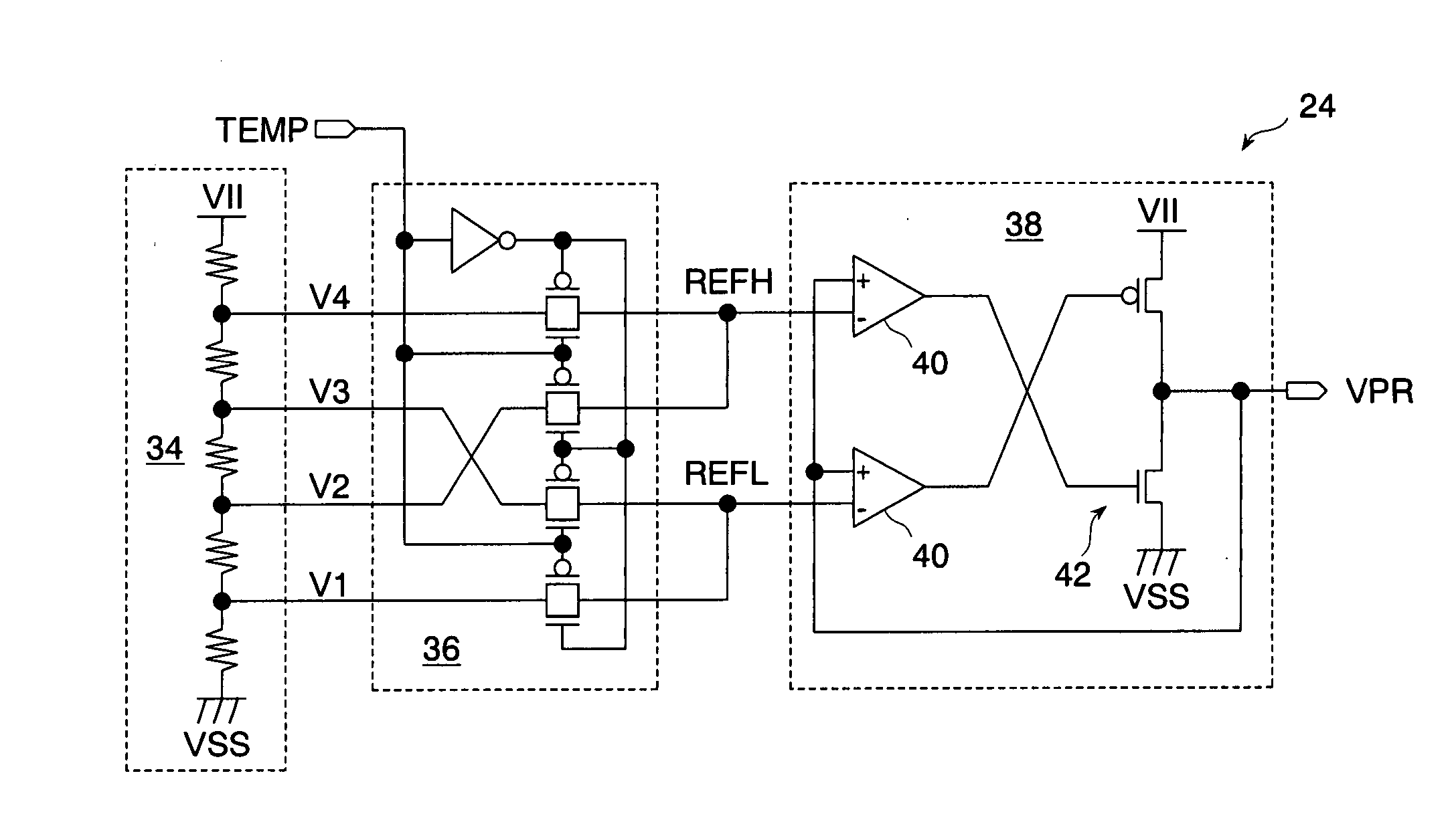
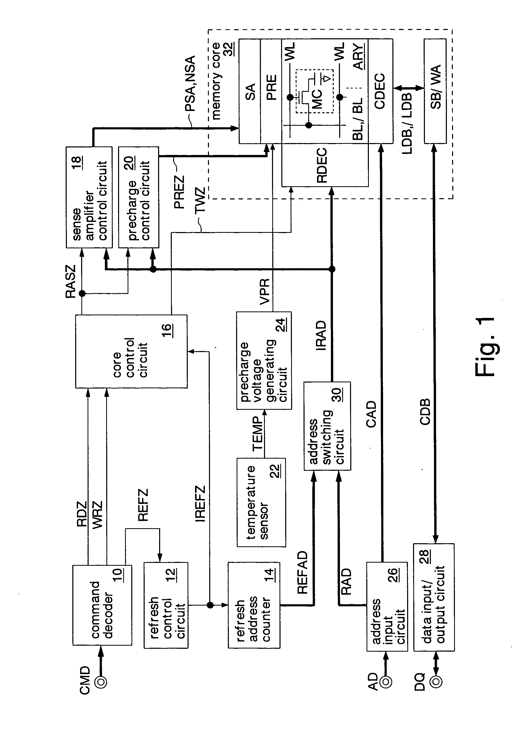
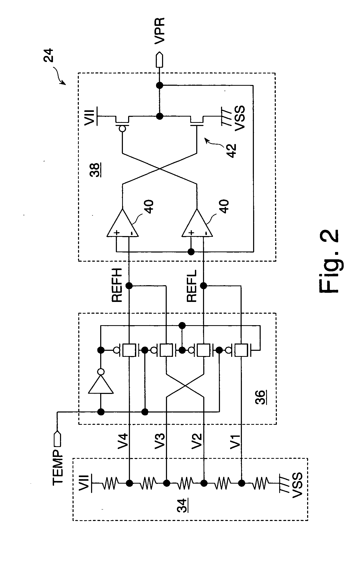
[0036]FIG. 1 shows the semiconductor memory of the invention. This semiconductor memory is formed as a dynamic RAM chip (hereinafter, “DRAM”) by using a CMOS process on a silicon substrate. The DRAM is used as, for example, a work memory which is mounted in a portable equipment such as mobile phone.

[0037] The DRAM includes a command decoder 10, a refresh control circuit 12, a refresh address counter 14, a core control circuit 16, a sense amplifier control circuit 18, a precharge control circuit 20, a temperature sensor 22, a precharge voltage generating circuit 24, an address input circuit 26, a data input / output circuit 28, an address switching circuit 30 and a memory core 32. Note that, in FIG. 1, only principal signals necessary for the description of the invention are shown.

[0038] The command decoder 10 receives a command signal CMD supplied from an external terminal (for example, a chip select signal / CS, a row address strobe signal / RAS, a column address strobe signal / CAS, a...

second embodiment

[0081]FIG. 10 shows the relationship between the data retaining time of the DRAM of the second embodiment and the temperature. A thick solid line indicates the data retaining time (worst) of the DRAM of the invention. In this example, the ambient temperature rises to successively shifts into the temperature zones TP1-TP4, and each time the ambient temperature exceeds boundary temperatures BT1, BT2 and BT3, the precharge voltage VPR changes from VPR1 to VPR2, from VPR2 to VPR3, and from VPR3 to VPR4 and lowers gradually.

[0082] In a case where the ambient temperature falls, reverse changes proceed. As thus far described, the same advantages as in the first embodiment can be attained also in the second embodiment. Further, the plurality of kinds of precharge voltages VPR1-VPR4 are switched in accordance with the ambient temperature, whereby the data retaining time can be lengthened more, and the frequency of refreshes can be lowered.

[0083]FIG. 11 shows the third embodiment of the semi...

fourth embodiment

[0091]FIG. 14 shows the operation of the memory core 32 in the case where the “1 data” is read from the memory cell MC, in the The same operations as in FIG. 4 shall be omitted from detailed description. The waveforms of the precharge signal PREZ, word line WL, and sense amplifier activating signals PSA and NSA are the same as in FIG. 4.

[0092] In this embodiment, the precharge voltage VPR is set to be high at the low temperature. The precharge voltage VPR is heightened at the low temperature, whereby the read margin of the “1 data” decreases. At a normal temperature and at a high temperature, the read margin of the “1 data” decreases due to the fall of the cell voltage STR attributed to the junction leak current. Accordingly, the difference between the read margins RM of the “1 data” at the low temperature and at the high temperature becomes small. Incidentally, at the low temperature, a leak current from the memory cell MC is very small, so that the read margin is originally suffi...


PUM


Abstract

A precharge voltage generating circuit outputs any of a plurality of kinds of precharge voltages in accordance with an ambient temperature. A precharge circuit supplies the precharge voltage to a bit line during the nonaccess of a dynamic memory cell. A sense amplifier amplifies a difference between the voltage of a data signal read from the dynamic memory cell onto the bit line and the supplied precharge voltage. The precharge voltage is altered in accordance with the ambient temperature, whereby the read margin of the sense amplifier can be changed, and the worst value of the data retaining time of the memory cell can be improved. As a result, the frequency of refreshing of the memory cell can be lowered, reducing power consumption and a standby current.

Description

CROSS REFERENCE TO RELATED APPLICATION [0001] This application is a continuation application of International Application PCT / JP 2004 / 008741, filed Jun. 22, 2004, and designating the U.S.BACKGROUND OF THE INVENTION [0002] 1. Field of the Invention [0003] The present invention relates to a technique for reducing the power consumption of a semiconductor memory which has dynamic memory cells that need to be cyclically refreshed. [0004] 2. Description of the Related Art [0005] A memory capacity necessary for a portable terminal such as mobile phone has been on the rise year by year. In this situation, a dynamic RAM (hereinafter, “DRAM” ) has come to be used as the work memory of the portable terminal instead of a conventional static RAM (hereinafter, “SRAM”). Since the DRAM is smaller than the SRAM in the number of elements constituting each memory cell, the chip size thereof can be made smaller, and the chip cost thereof can be made lower than that of the SRAM. [0006] On the other hand...

Claims


Application Information

Patent Timeline
IPC IPC(8): G11C11/34G11C7/04G11C7/12G11C11/403G11C11/406G11C11/409G11C11/4094
CPCG11C7/04G11C7/12G11C11/406G11C11/40626G11C11/4094G11C2211/4068
Inventor NISHIMURA, KOICHIIKEMASU, SHINICHIRO
Owner SOCIONEXT INC
Why Eureka
Try Eureka