Solar cell module

a solar cell and module technology, applied in the field of solar cell modules, can solve the problems of reducing long-term reliability, weak physical shock of solar cells, and inability to sufficiently extract or reduce output, so as to achieve the effect of increasing the breaking strength

Inactive Publication Date: 2007-05-03
KYOCERA CORP
View PDF12 Cites 82 Cited by
  • Summary
  • Abstract
  • Description
  • Claims
  • Application Information

AI Technical Summary

Benefits of technology

[0171] The sample No. 2 is a sample outside the scope of the present invention in which the edges of all the bus bar electrodes 4a and 5a are coated with the solder 6, and are not brought into direct contact with the EVA which is the filler 10 or are not brought into contact therewith through the solder resist 7. The breaking strength was 15 N, and the rate of incidence of micro cracks was 50%, which were unsatisfied results.
[0172] The sample No. 3 is a solar cell module completed as a result of coating only the center portions of the bus bar electrodes 4a and 5a with the solder 6 to weld the center portion of the inner lead 8. The sample has the form shown in FIG. 5 according to the present invention in which the edges of the bus bar electrodes and the filler 10 are brought into direct contact with each other. In this case, the breaking strength of the solar cell was 23 N, and the rate of incidence of micro cracks was 0%, so that the effect of the invention was confirmed.
[0173] The sample No. 4 is a sample in which the bus bar electrodes 4a and 5a are not coated with the solder 6. A solar cell module completed as a result of utilizing the solder with which the inner lead 8 is coated to weld the center portion of the inner lead 8 has the form shown in FIG. 5 according to the present invention in which the edges of the electrodes and the filler 10 are brought into d

Problems solved by technology

Therefore, the solar cell is weak in physical shock, and must be protected from rain or the like when the solar cell is mounted outdoors.
The stresses cause some problems.
For example, defects such as micro cracks occur in the silicon substrate 1 near the bus bar electrode 5a, which develop into a large craze in the subsequent manufacturing process.
Further, an output cannot be sufficiently extracted or is lowered.
Therefore, micro cracks

Method used


Image

  • Solar cell module
  • Solar cell module
  • Solar cell module

Examples


example 1

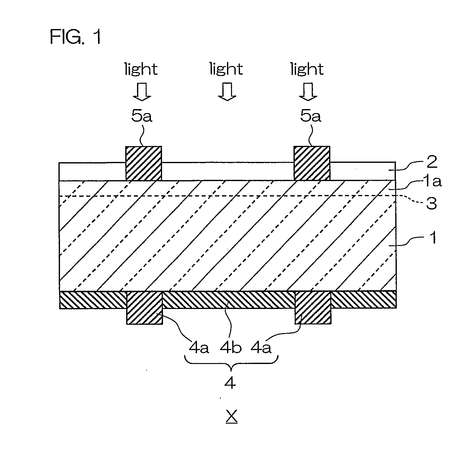
[0157] A damage layer on a surface of a p-type polycrystalline silicon substrate 1 having an outer shape of 15 cm×15 cm and having a relative resistance of 1.5 Ω·cm was etched and cleaned by an alkali. The silicon substrate 1 was then arranged in a diffusion furnace, and was heated in phosphorous oxychloride (POCl3), thereby diffusing a phosphorous atom on the surface of the silicon substrate 1 so as to have a concentration of 1×10¹⁷ atoms / cm3, to form an n-type diffusion layer 1a. A silicon nitride film having a thickness of 850 Å serving as an anti reflection film 2 was formed thereon by a plasma CVD method.

[0158] In order to form a back surface current collecting electrode 4b on a back surface of the silicon substrate 1, an aluminum paste produced in a paste shape by respectively adding 20 parts by weight and 3 parts by weight of an organic vehicle and a glass flit to 100 parts by weight of an aluminum powder was applied and dried by a screen printing method. In order to form a ...

example 2

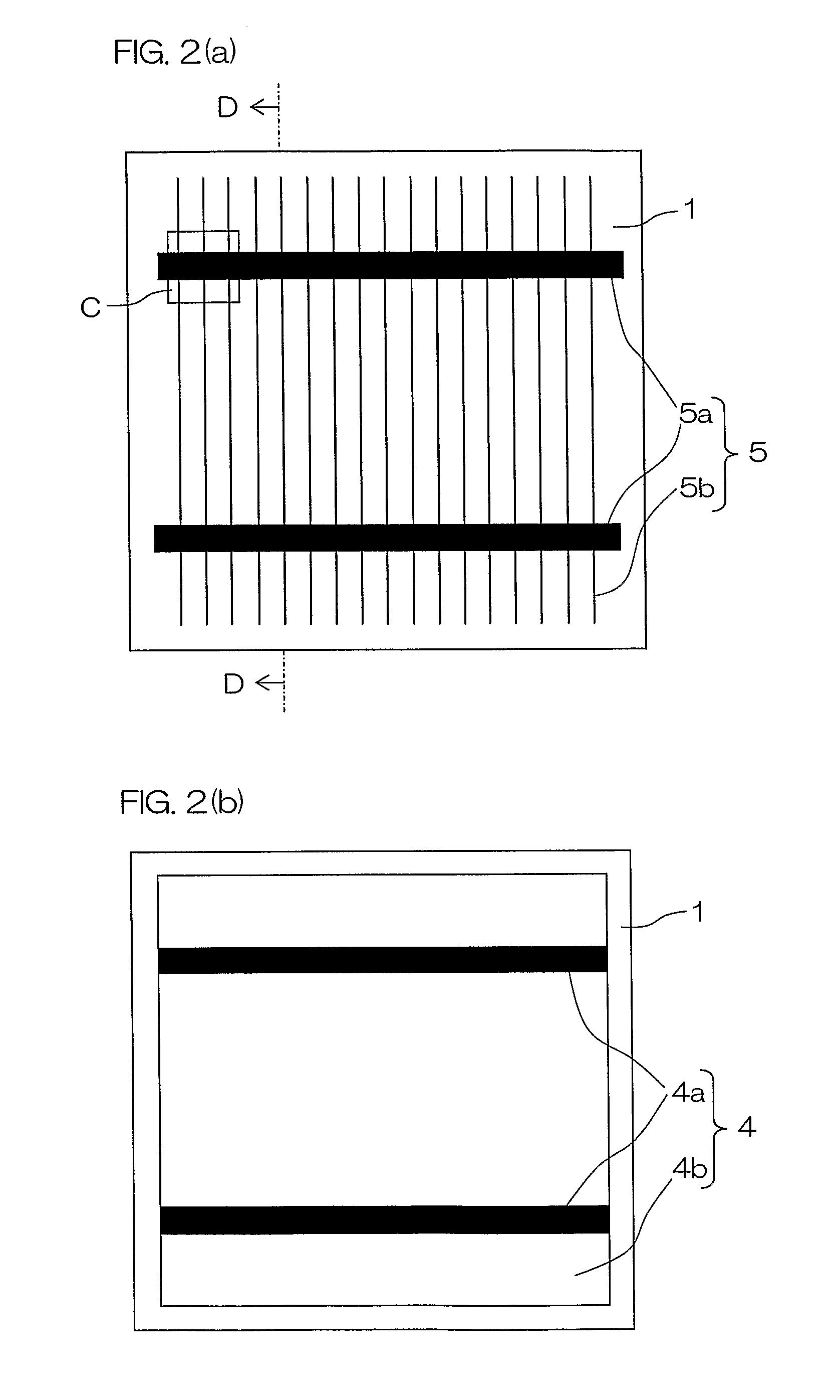
[0176] Solar cells were formed in the same manner as that in the example 1. Thereafter, a solder resist was printed and applied with a pattern shown in FIG. 8 (b) to an area, on the side of a surface finger electrode 5b from one end at which the surface finger electrode 5b is connected to a surface bus bar electrode 5a to a distance of 1 mm therefrom and was thermoset, to form a coating member 14′. Thereafter, the inner lead 8 using a copper foil coated with a solder was thermally welded. In this case, an attempt to intentionally shift the position of the inner lead 8 to make the inner lead 8 jut out of the surface bus bar electrode 5a to intentionally connect them with a solder is made. However, with respect to a sample in which the coating member 14′ which is a solder resist is provided, they were not connected to each other in any way. Further, with respect to a sample in which the coating member 14′ is not provided, they are joined to each other in a case where a flux is applied...

example 3

[0185] Solar cells were formed in the same manner as that in the example 1.

[0186] An inner lead 8 using a copper foil having a width of 2 mm and having a thickness of 200 μm which is provided with a solder layer having a thickness of approximately 30 μm was then affixed by thermal welding such as hot-air welding over the whole lengths of bus bar electrodes 5a and 4a to which a flux was applied, to connect and wire the above-mentioned solar cells.

[0187] At this time, the composition of the solder was changed into a plurality of types of compositions. Solders used for samples No. 21 to 28 are ones composed of 1 to 90% by weight of Bi, 2% by weight of Ag, and the remaining percent by weight of Sn. Solders used for samples No. 29 to 32 are ones composed of 50% by weight of Bi, 0.1 to 9% by weight of Ag, and the remaining percent by weight of Sn. A solder in a sample No. 33 has a composition of Sn-5Ag-0.5Cu, a solder in a sample No. 34 has a composition of Sn-5Ag-0.5Cu, and a solder in...


PUM


Abstract

The largest stress is created in the vicinity of the boundary between an edge of a bus bar electrode in a solar cell and a surface of a semiconductor substrate, and stress are easily concentrated. Accordingly, defects such as micro cracks occur in the semiconductor substrate, which develop into a large craze with the defects as its starting point. In connecting bus bar electrodes 4a and 5a in the solar cell by an inner lead 8, therefore, a solder 6 is not brought into contact with edges along the longitudinal direction if the bus bar electrodes 4a and 5a and portions F from the edges to a predetermined distance a inward therefrom, and is brought into direct contact with a filler 10.

Description

TECHNICAL FIELD [0001] The present invention relates to a solar cell module, and more particularly to a solar cell module in which a plurality of solar cells each having an electrode formed therein are connected to a semiconductor substrate by an inner lead. BACKGROUND ART [0002] A solar cell is produced using a single crystalline silicon substrate or a polycrystalline silicon substrate. Therefore, the solar cell is weak in physical shock, and must be protected from rain or the like when the solar cell is mounted outdoors. Since one solar cell hardly generates electrical output, a plurality of solar cells must be connected in series so that practical electrical output can be extracted. [0003] Therefore, a method of connecting a plurality of solar cells, interposing the connected solar cells between translucent panel and a back surface protect member, and sealing a filler mainly composed of an ethylene vinyl acetate copolymer (EVA) or the like among the solar cells, to produce a sola...

Claims


Application Information

Patent Timeline
IPC IPC(8): H02N6/00H01L31/042H01L31/048H01L31/05
CPCH01L31/0512Y02E10/50H01L31/0508H01L31/042
Inventor FUJII, SHUICHIKANEKO, TOSHIHIKOTSUGE, TAKASHISHIRASAWA, KATSUHIKO
Owner KYOCERA CORP
Why Eureka
Try Eureka