System, method, and apparatus for providing a temporary, deep shunt on wafer structures for electrostatic discharge protection during processing

a technology of electrostatic discharge protection and wafer structure, which is applied in the field of protecting wafer-based structures from electrostatic discharge, can solve the problems of destroying or severely damaging the read sensor, the slider material has very low electrical conductivity, and cannot function as a seed layer, and achieves easy formation, easy removal, and sufficient esd protection

Inactive Publication Date: 2007-05-03
WESTERN DIGITAL TECH INC
View PDF17 Cites 15 Cited by
  • Summary
  • Abstract
  • Description
  • Claims
  • Application Information

AI Technical Summary

Benefits of technology

[0012] One embodiment of a system, method, and apparatus for the present invention, a temporary, easily formed shunt is formed on a sensor during wafer processing without requiring additional wafer processing or fabrication. The shunt is also easily removed very late in the sensor forming process and thereby protects the sensor during most of the sensor formation steps. The shunt can be defined at various levels of resistance and provides sufficient ESD protection and superior cost benefits to the proposed laser delete technology.

Problems solved by technology

A discharge with only a few volts between the spaced apart first and second read pads can destroy or severely damage the read sensor.
The slider material has very low electrical conductivity and therefore cannot function as a seed layer for plating the pads of the conductive shunt (if plated).
Gold is a desirable material for the conductive shunt but has very poor adhesion to the aluminum oxide overcoat.
Also, adhesion between patterning resist and gold is poor.
One proposed solution is to use laser delete shunts, which are relatively expensive and require difficult manufacturing steps.

Method used


Image

  • System, method, and apparatus for providing a temporary, deep shunt on wafer structures for electrostatic discharge protection during processing
  • System, method, and apparatus for providing a temporary, deep shunt on wafer structures for electrostatic discharge protection during processing
  • System, method, and apparatus for providing a temporary, deep shunt on wafer structures for electrostatic discharge protection during processing

Examples


Embodiment Construction

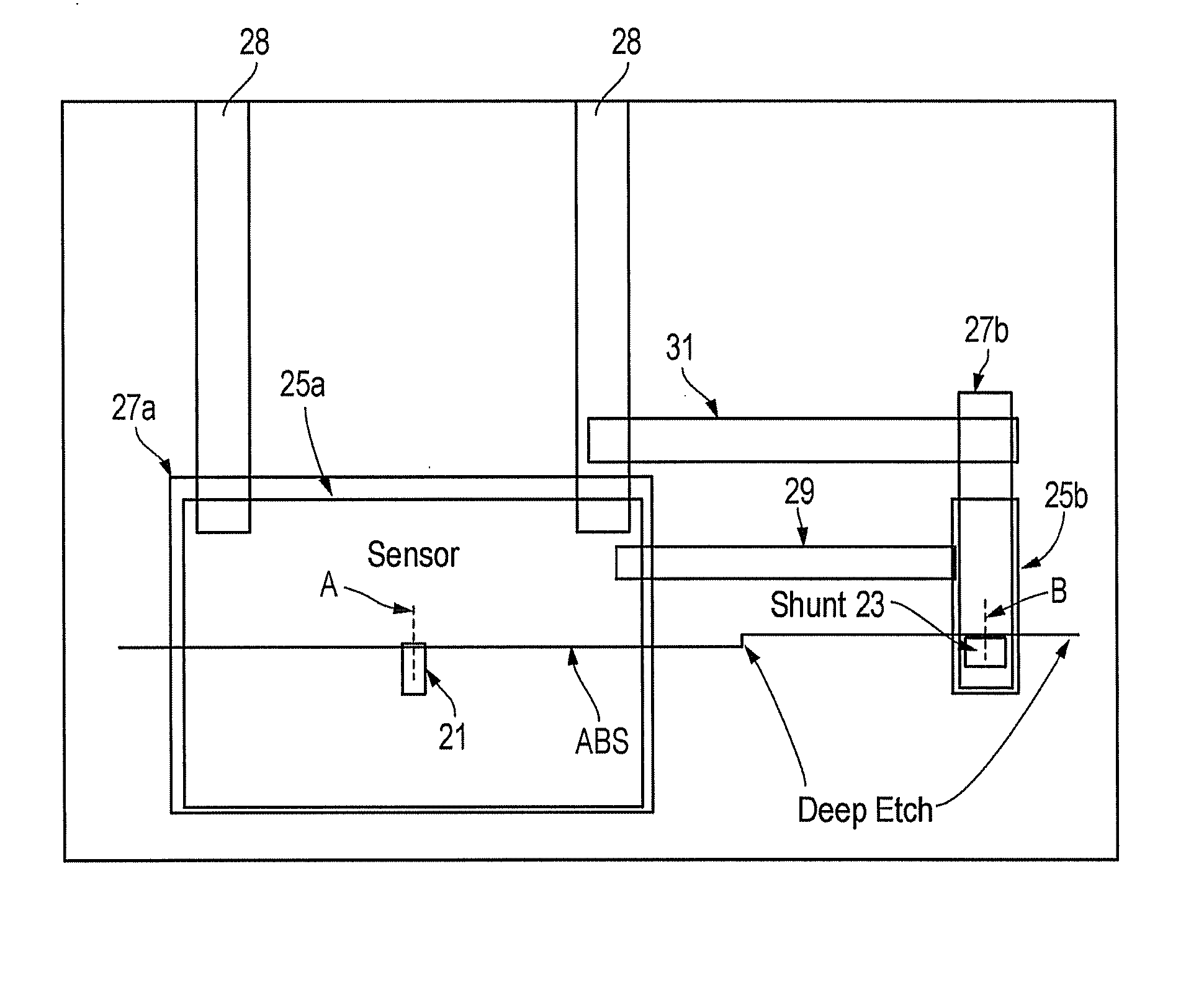
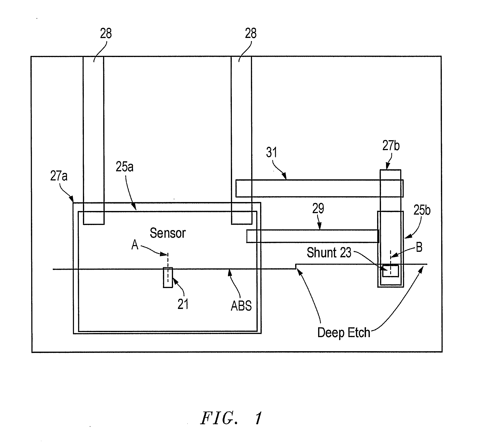
[0032] Referring to FIG. 1, a schematic representation of one embodiment of a series of mask overlays of an electrical sensor (e.g., GMR or TMR) design that incorporates a temporary, wafer level shunt constructed in accordance with the present invention is shown. The relatively low resistance shunt is designed to protect electrically sensitive components (e.g., the sensor) from electrical damage, such as electrostatic discharge, while the sensor and structure are being fabricated during various wafer and slider processing steps.

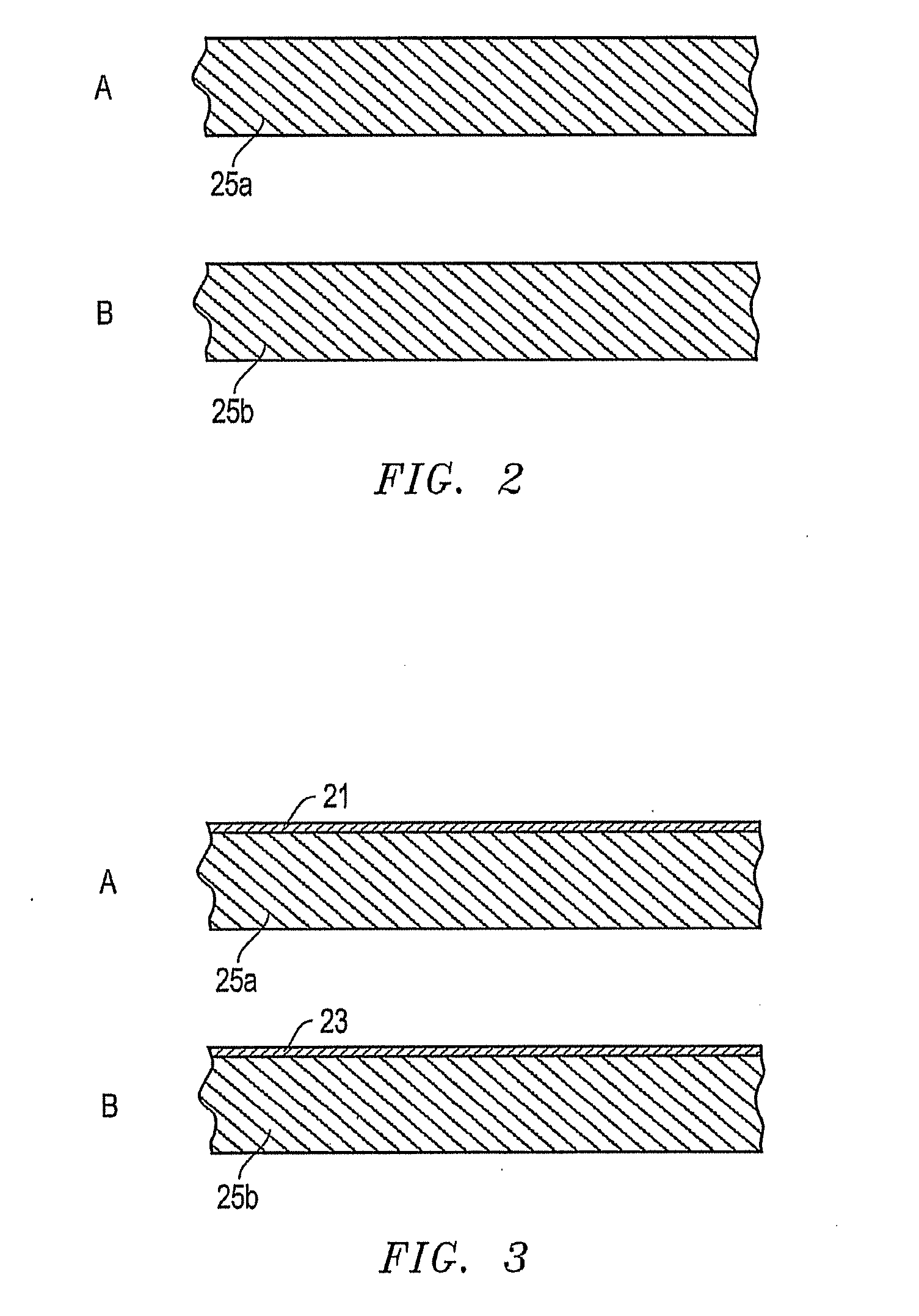
[0033]FIG. 1 illustrates the build of a critical region of the design, including a sensor 21, which is located in a sensor region “A”, and a shunt 23, which is located in a deep depth (e.g., deep etch) region “B”. A significant advantage of the present invention is that the sensor 21 and shunt 23 can be built simultaneously to reduce cost. In one embodiment, the sensor has a pair of electrically conductive leads that are initially formed as first and second ...


PUM

PropertyMeasurementUnit
depthaaaaaaaaaa
depthaaaaaaaaaa
electrically sensitiveaaaaaaaaaa

Abstract

A method of temporarily protecting an electrically sensitive component from damage due to electrostatic discharge includes defining a shunt having first and second leads electrically connected in parallel with the component and separated by a gap. A portion of a shield layer is deposited to form the shunt between the first and second leads to span the gap therebetween and form a shunted assembly. The shunted assembly and component are lapped to form the ABS at the location of the component, a sacrificial carbon overcoat is deposited on the ABS, and additional processing is performed on the shunted assembly. A portion of the shunted assembly, the shunt, and portions of the sacrificial carbon overcoat are then removed to form an electrical open for an unshunted assembly having ABS features comprising an air bearing cavity/deep gap at a former location of the shunted assembly.

Description

[0001] This patent application is a continuation-in-part of and claims priority to U.S. patent application Ser. No. 11,029,134, filed on Jan. 4, 2005, which is incorporated herein by reference.BACKGROUND OF THE INVENTION [0002] 1. Technical Field [0003] The present invention relates in general to protecting wafer-based structures from electrostatic discharge and, in particular, to an improved system, method, and apparatus for forming and then later removing a temporary, deep shunt on a wafer structure that protects the electrically sensitive structure during fabrication. [0004] 2. Description of the Related Art [0005] Magnetic disk drives include a rotating magnetic disk, a slider that has read and write heads, a suspension arm above the rotating disk and an actuator arm that swings the suspension arm to place the read and write heads over selected circular tracks on the rotating disk. The suspension arm urges the slider into contact with the surface of the disk when the disk is not...

Claims


Application Information

Patent Timeline
Patent Type & Authority Applications(United States)
IPC IPC(8): G11B5/33B44C1/22B24B1/00G11B5/127
CPCG11B5/11G11B5/3163G11B5/3903Y10T29/49041G11B5/455Y10T29/49046Y10T29/49043G11B5/40G11B5/3173G11B5/6094B24B1/00
Inventor SEAGLE, DAVID JOHN
Owner WESTERN DIGITAL TECH INC
Why Eureka
Try Eureka