Method of manufacturing semiconductor device

Inactive Publication Date: 2007-05-03
KK TOSHIBA
View PDF4 Cites 5 Cited by
  • Summary
  • Abstract
  • Description
  • Claims
  • Application Information

AI Technical Summary

Problems solved by technology

However, there is a limit to the scaling of the gate insulating film in a device of the 0.1 μm generation and later.
This results from actualization of an increase of gate leakage current due to tunnel current as the gate insulating film gets thinner.
Further, in this generation, depletion of the gate electrode cannot be ignored, and it became difficult to achieve a decreased effective thickness of the gate insulating film.
Specifically, as shown in the ITRS Road Map of 2003, it is difficult to implement a transistor with a conventional polycrystalline silicon electrode in a physical film thickness region of less than 1.0 nm.
However, a sufficient inspection of characteristics including reliability of these materials, like that of the conventional silicon oxide film, has not been done.

Method used


Image

  • Method of manufacturing semiconductor device
  • Method of manufacturing semiconductor device
  • Method of manufacturing semiconductor device

Examples


example 1

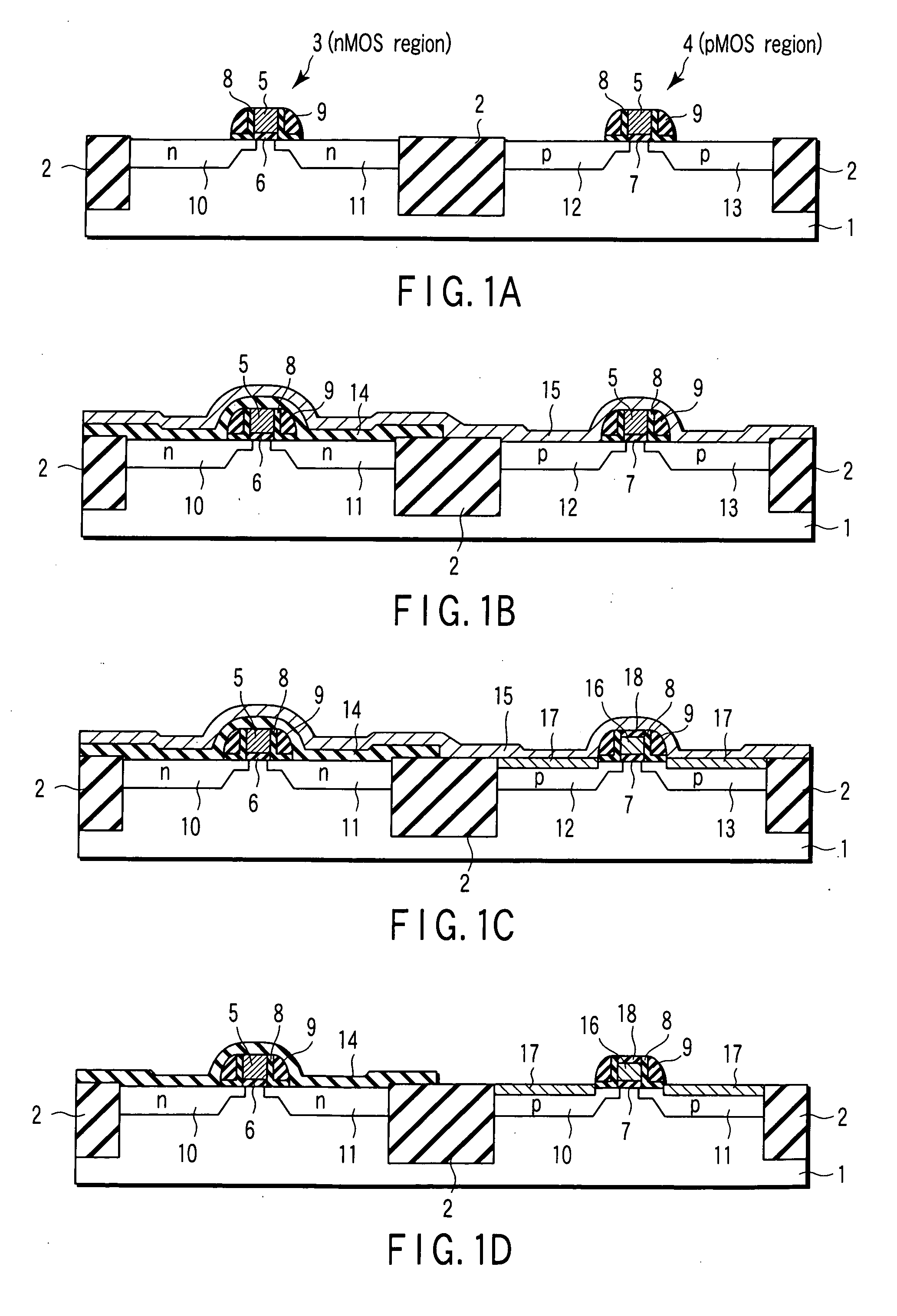
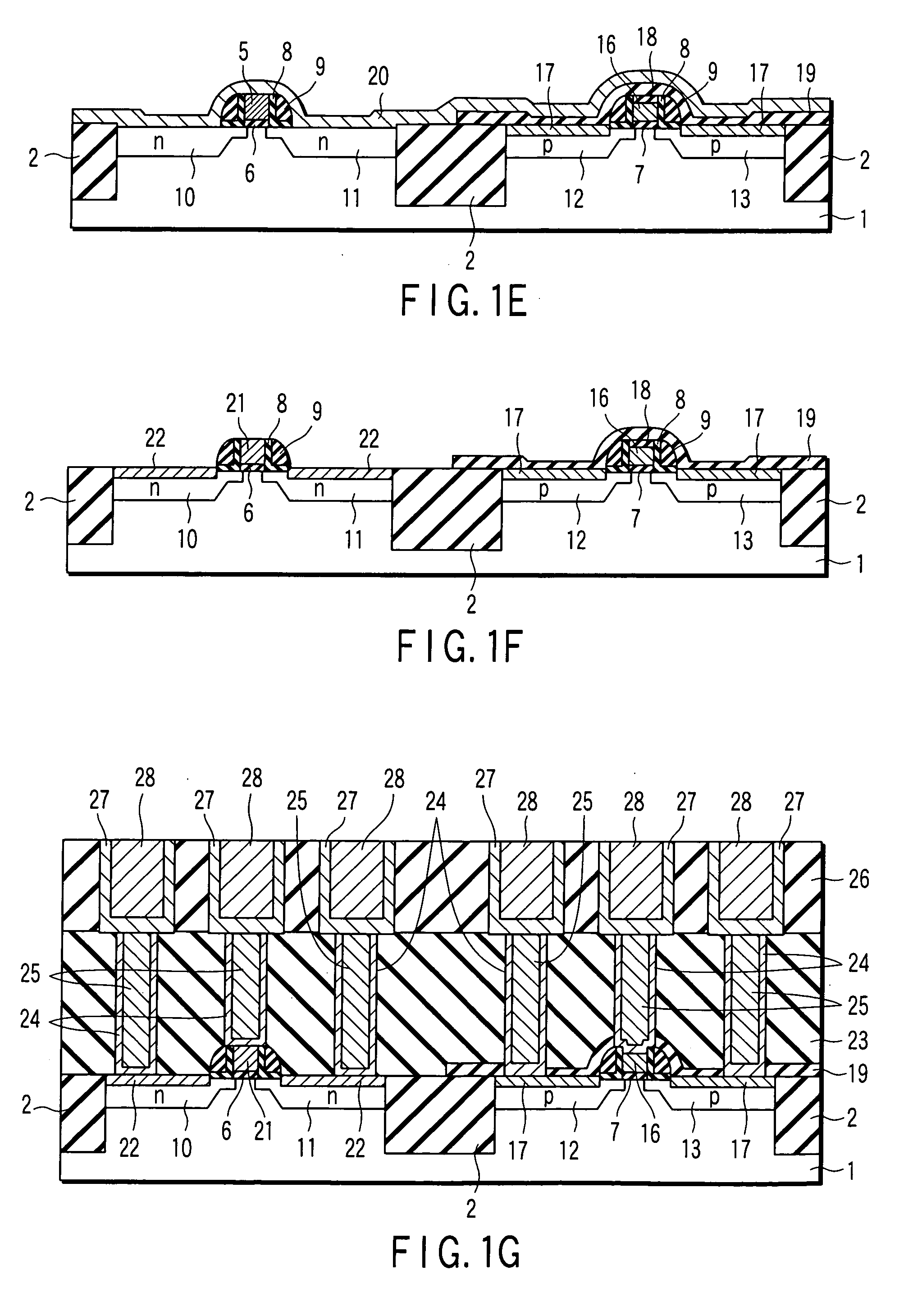
[0056]FIGS. 1A to 1G are cross-sectional views each showing the steps of manufacturing a CMOS transistor in Example 1, and FIGS. 2A to 2F are longitudinal sectional views of gate electrodes shown in FIGS. 1A to 1F.

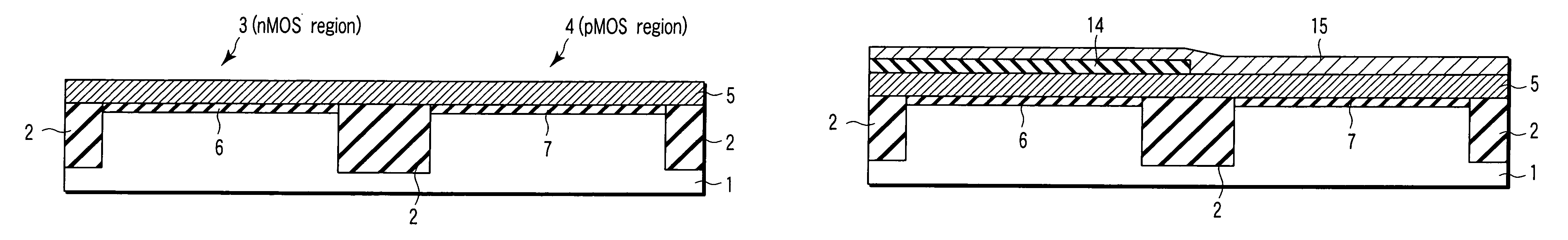
[0057] First, by forming an element isolator 2 on a single crystal silicon substrate 1 as shown in FIGS. 1A and 2A, the surface of the single crystal silicon substrate 1 was isolated into a plurality of an n-MOS region 3 and a p-MOS region 4. Then, a gate insulating film such as a silicon oxynitride film was formed on the single crystal silicon substrate 1 located in the n-MOS region 3 and the p-MOS region 4 respectively, and a polycrystalline silicon film was deposited all over the surface. Subsequently, the polycrystalline silicon film was etched anisotropically using a resist pattern as a mask to form a plurality of electrode patterns 5. The silicon oxynitride film is removed by etching selectively using these electrode patterns 5, whereby gate insulating films 6 and 7...

example 2

[0065]FIGS. 3A to 3H are cross-sectional views each showing the steps of manufacturing a CMOS transistor in Example 2.

[0066] First, by forming an element isolator 32 on a single crystal silicon substrate 31 as shown in FIG. 3A, the surface of the single crystal silicon substrate 31 was isolated into a plurality of an n-MOS region 33 and a p-MOS region 34. Then, a gate insulating film such as a silicon oxynitride film was formed on the single crystal silicon substrate 31 located in the n-MOS region 33 and the p-MOS region 34 respectively, and a polycrystalline silicon film and a silicon oxide film were deposited successively all over the surface. Subsequently, the silicon oxide film was etched anisotropically using a resist pattern as a mask to form a plurality of silicon oxide patterns 35. The polycrystalline silicon film underneath the silicon oxide pattern was etched anisotropically using these silicon oxide patterns 35 as a mask, whereby a plurality of electrode patterns 36 were...


PUM


Abstract

The present invention provides a method of manufacturing a semiconductor device, comprising forming an electrode pattern made of silicon on a gate insulating film in an n-MOS region and a p-MOS region of a semiconductor substrate, masking the n-MOS region including the first electrode pattern with a first insulating film pattern, forming a first metal film made of platinum all over the surface, forming a gate electrode consisting of a platinum silicide in the p-MOS region, forming an silicon oxide film on the surface of the gate electrode by oxidation, dissolving away a non-reacting Pt film, removing the first insulating film pattern, masking the p-MOS region including the electrode pattern with a second insulating film pattern, forming a second metal film made of europium all over the surface, and forming a gate electrode consisting of a europium silicide in the n-MOS region.

Description

CROSS-REFERENCE TO RELATED APPLICATIONS [0001] This application is based upon and claims the benefit of priority from prior Japanese Patent Application No. 2005-313258, field Oct. 27, 2005, the entire contents of which are incorporated herein by reference. BACKGROUND OF THE INVENTION [0002] 1. Field of the Invention [0003] The present invention relates to a method of manufacturing a semiconductor device. [0004] 2. Description of the Related Art [0005] In MOSFET technology, device miniaturization has proceeded to achieve higher performance. However, there is a limit to the scaling of the gate insulating film in a device of the 0.1 μm generation and later. This results from actualization of an increase of gate leakage current due to tunnel current as the gate insulating film gets thinner. Further, in this generation, depletion of the gate electrode cannot be ignored, and it became difficult to achieve a decreased effective thickness of the gate insulating film. Specifically, as shown ...

Claims


Application Information

Patent Timeline
IPC IPC(8): H01L21/336
CPCH01L21/28518H01L21/823835H01L29/665H01L29/6656H01L29/6659H01L29/7833
Inventor NAKAJIMA, KAZUAKIYAGISHITA, ATSUSHI
Owner KK TOSHIBA
Why Eureka
Try Eureka