Small Scanned Magentron

a magentron and small technology, applied in the field of materials sputtering, can solve the problems of high temperature operation with possible damage, severely affect the performance and reliability of the resulting device, and the sputtering is not inherently adapted to sidewall coverage, etc., to achieve complete target utilization, increase plasma density, and increase the effect of uniformity of sputtering

US20070102284A1Inactive Publication Date: 2007-05-10APPLIED MATERIALS INC
12 Cites 2 Cited by

Patent Information

Authority / Receiving Office
US · United States
Patent Type
Applications(United States)
Current Assignee / Owner
Publication Date
2007-05-10
Estimated Expiration
Not applicable · inactive patent

Smart Images

  • Figure 1
    Figure 1
  • Figure 2
    Figure 2
  • Figure 3
    Figure 3
Patent Text Reader

Abstract

A small magnet assembly having a magnet assembly of area less than 10% of the target area, is scanned in a retrograde planetary or epicyclic path about the back of a target being plasma sputtered including an orbital rotation about the center axis of the target and a planetary rotation about another axis rotating about the target center axis. The magnet assembly passes through the target center, thus allowing full target coverage. A properly chosen ratio of the two rotations about respective axes produces a much slower magnet velocity near the target periphery than at the target center. A geared planetary mechanism includes a rotating drive plate, a fixed center gear, and an idler and a follower gear rotatably supported in the drive plane supporting a cantilevered magnet assembly on the side of the drive plate facing the target.
Need to check novelty before this filing date? Find Prior Art

Description

RELATED APPLICATION

[0001] This application is a continuation Ser. No. 10 / 862,257, filed Jun. 7, 2004, for which a Notice of Allowance has been received, which is a continuation of Ser. No. 10 / 152,494, filed May 21, 2002, now issued as U.S. Pat. No. 6,841,050.FIELD OF THE INVENTION

[0002] The invention relates generally to sputtering of materials. In particular, the invention relates to the magnetron creating a magnetic field to enhance plasma sputtering. BACKGROUND ART

[0003] Sputtering, alternatively called physical vapor deposition (PVD), is commonly used in the fabrication of semiconductor integrated circuits for depositing layers of metals and related materials particularly for the formation of electrical interconnections. Somewhat older integrated circuit technology uses aluminum for horizontal interconnects and for vertical interconnects between metallization levels through vias having relatively modest aspect ratios. Such applications require fast deposition rates and high u...

Examples

Embodiment Construction

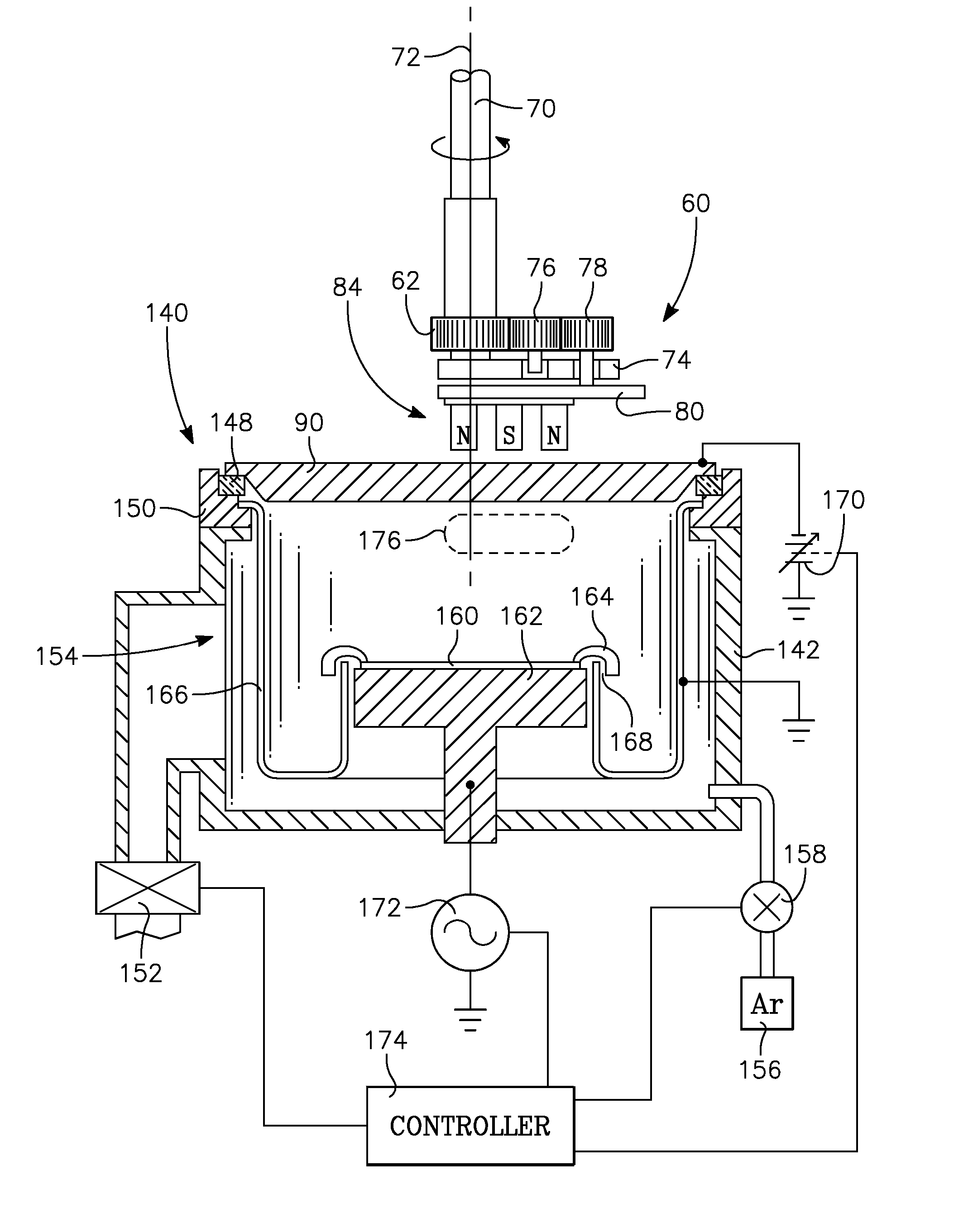
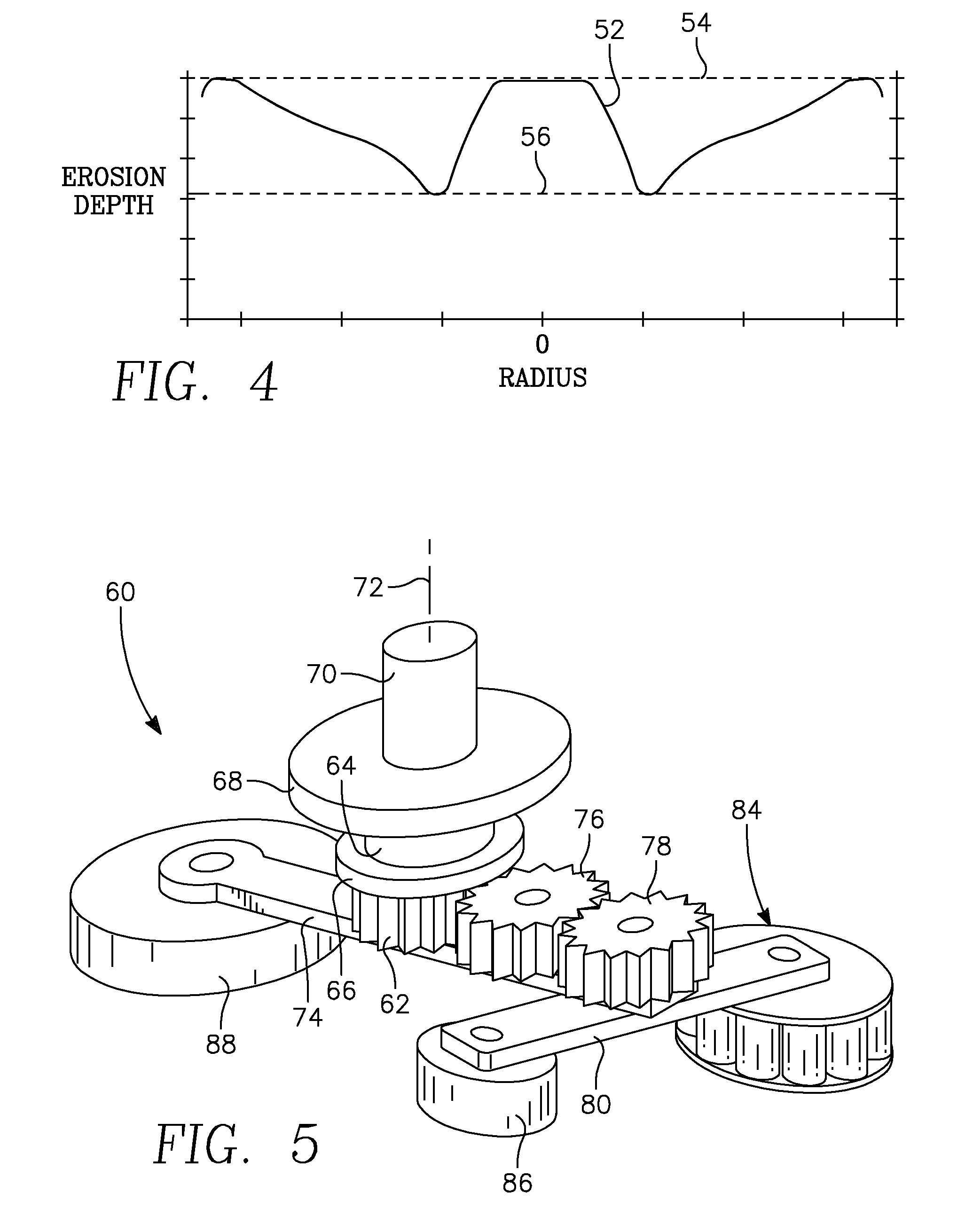
[0045] One principal embodiment of the invention relies upon a planetary mechanism, for instance, one using a planetary gear system, to allow a small circularly symmetric magnetron to fully cover the sputtering target. The planetary mechanism produces a planetary motion similar to that of a planet orbiting the sun while it is simultaneously executing planetary rotation about its own polar axis. For use with a magnetron, the planetary axis is parallel to but displaced from the orbital axis and the orbit is circular about the orbital axis. The magnet assembly of the magnetron is displaced from and rotates about the planetary axis while the planetary axis orbits or rotates about the orbital axis, thereby producing a complex trajectory for the magnetron. In retrograde planetary motion, the direction of planetary rotation is the reverse to the direction of orbital rotation.

[0046] In one geared embodiment illustrated in the orthographic view of FIG. 5, a magnetron assembly 60 includes a ...