

Organic electronic device
- Summary
- Abstract
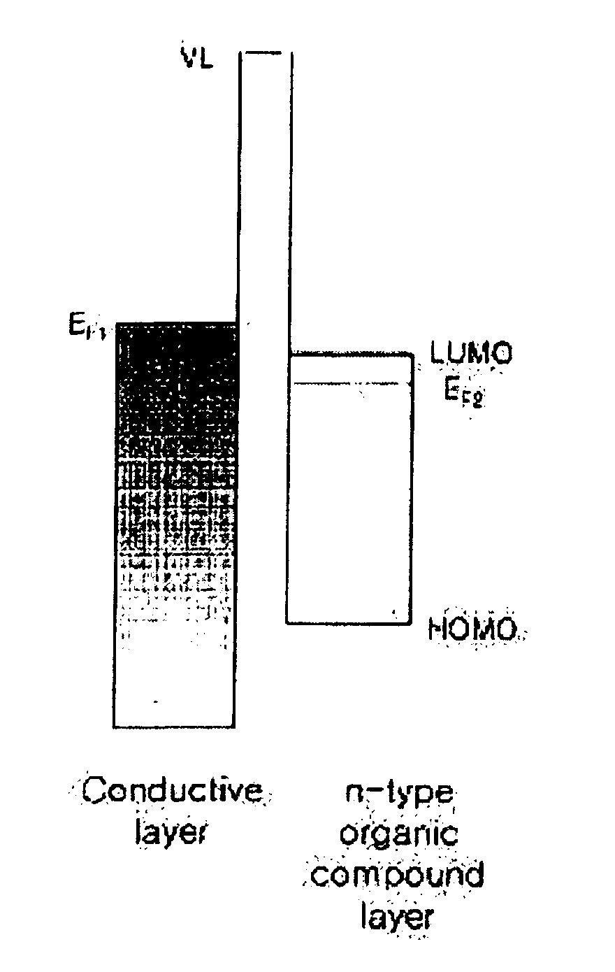
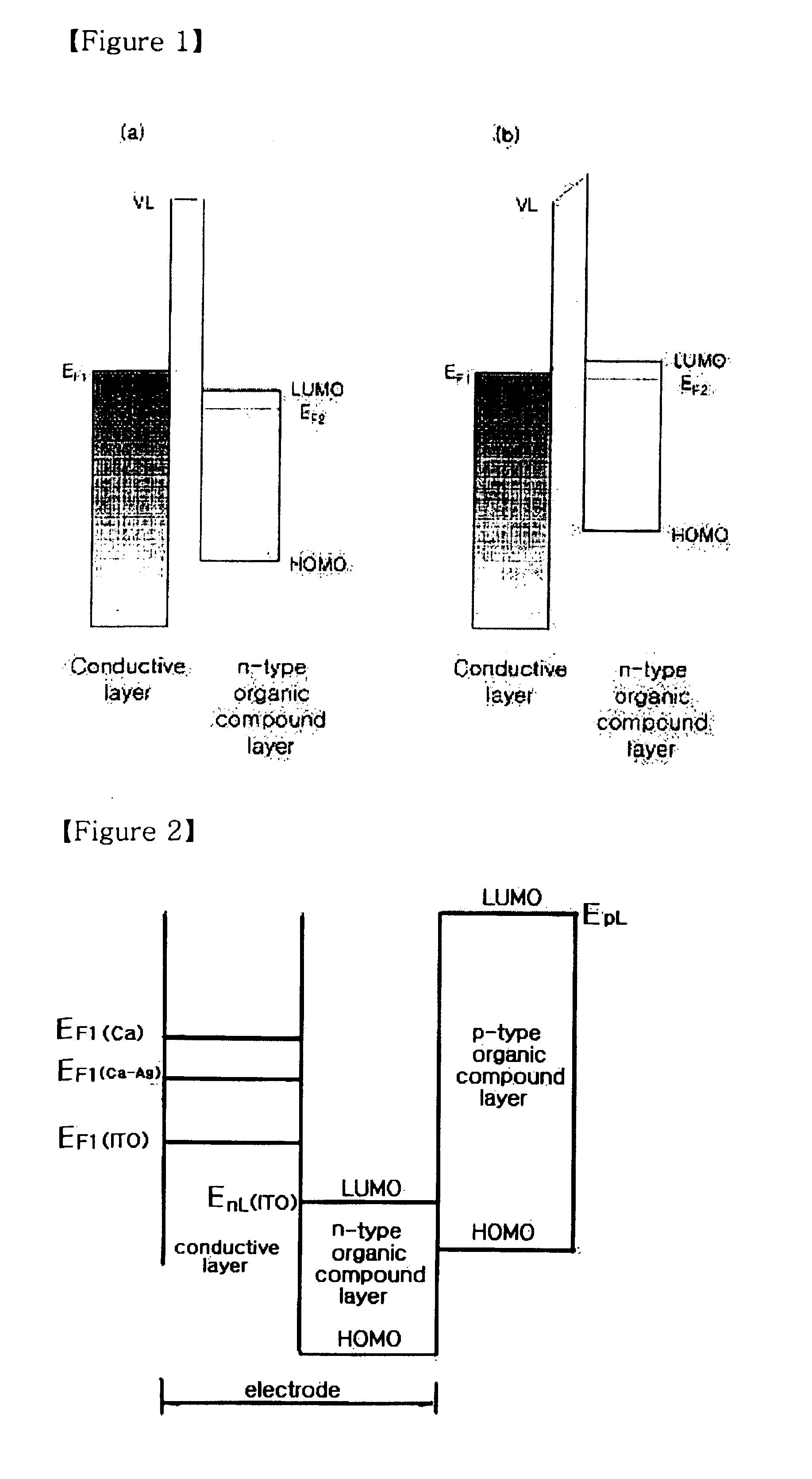
- Description
- Claims
- Application Information
AI Technical Summary
Benefits of technology
Problems solved by technology
Method used
Image

Examples
example 1
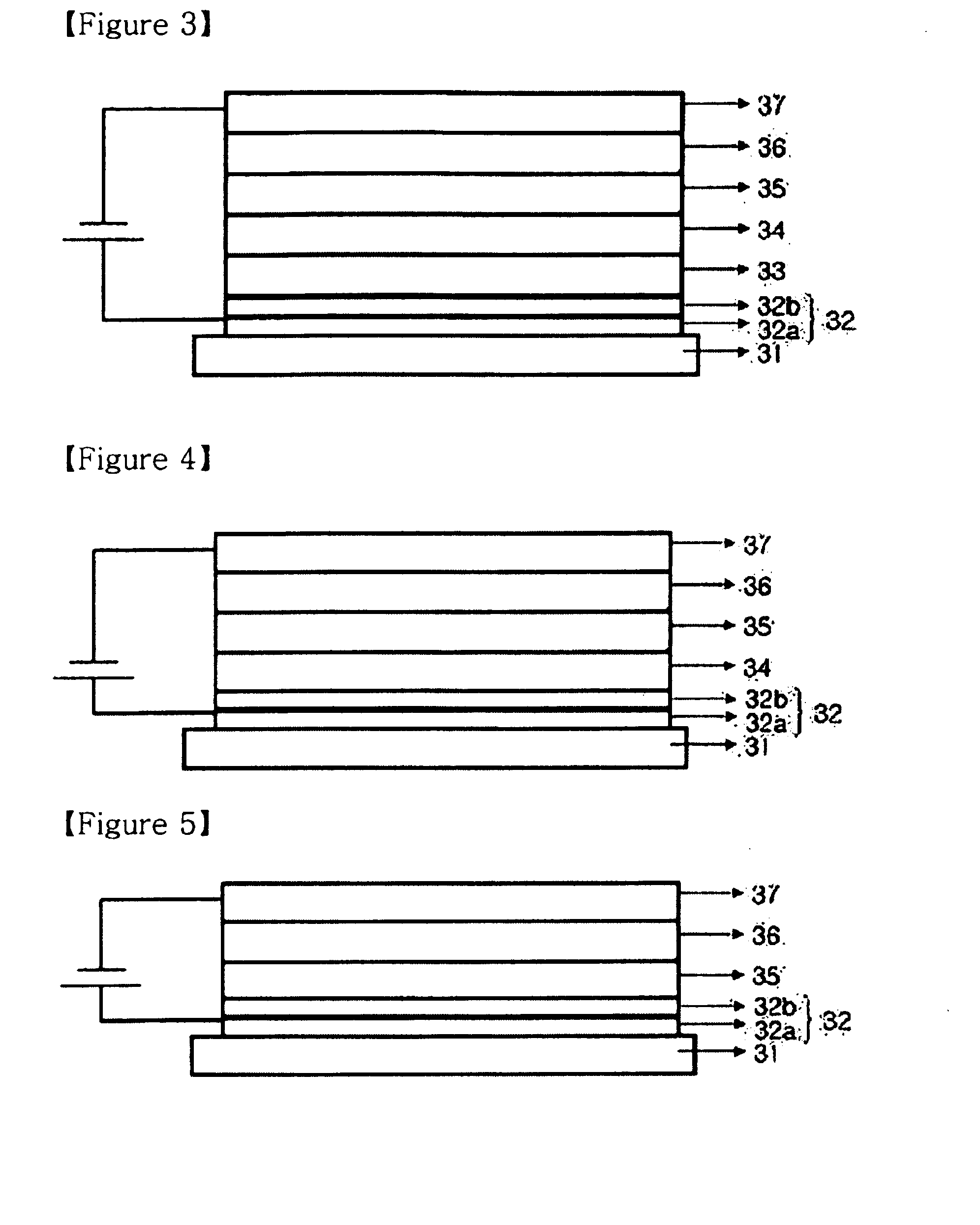
[0129] Organic Light Emitting Device Including Anode Having IZO—Ca Conductive Layer and HAT n-Type Organic Compound Layer
[0130] IZO was vacuum-deposited on a washed glass substrate to have a thickness of 1000 Å using a sputtering deposition apparatus and Ca was thermally vacuum-deposited thereon to have a thickness of 100 Å. As a result, a transparent IZO—Ca conductive layer having a work function of 2.6 eV was formed. Then, HAT was thermally vacuum-deposited on the formed conductive layer to have a thickness of approximately 500 Å. As a result, a transparent anode having the IZO—Ca conductive layer and the HAT n-type organic compound layer was formed. Subsequently, 4,4′-bis[N-(1-naphthyl)-N-phenylamino]biphenyl (NPB) was vacuum-deposited on the anode to have a thickness of approximately 400 Å so as to form a p-type hole transport layer. Next, Alq3 having an HOMO energy level of approximately 5.7 eV was vacuum-deposited on the p-type hole transport layer to have a thickness of appr...
example 2
[0132] Organic Light Emitting Device Including Anode Having Ag—Ca Conductive Layer and HAT n-Type Organic Compound Layer
[0133] An organic light emitting device was manufactured by the same method as Example 1, except that Ag was thermally vacuum-deposited on a washed glass substrate to have a thickness of 200 Å and Ca was thermally vacuum-deposited thereon to have a thickness of 200 Å so as to form a semitransparent Ag—Ca conductive layer having a work function of 2.6 eV, instead of the transparent IZO—Ca conductive layer.
TABLE 1Work@50 mA / cm2@100 mA / cm2functionVoltageLuminanceVoltageLuminanceAnodeof anode(V)(cd / sq)(V)(cd / sq)Example 1IZO(1000 Å)2.6 eV5.1013006.302663—Ca(100 Å)Example 2Ag(200 Å)2.6 eV4.205004.801000—Ca(200 Å)
[0134] From Table 1 representing the luminance of Examples 1 and 2 depending on a current density and a voltage, it can be seen that holes are smoothly injected to the hole transport layer even though the energy difference between the LUMO energy level (approx...
PUM
| Property | Measurement | Unit |
|---|---|---|
| Area | aaaaa | aaaaa |
| Energy level | aaaaa | aaaaa |
| Length | aaaaa | aaaaa |
Abstract
Description
Claims
Application Information