High light extraction efficiency light emitting diode (LED)

Inactive Publication Date: 2007-05-10
RGT UNIV OF CALIFORNIA +1
View PDF53 Cites 160 Cited by
  • Summary
  • Abstract
  • Description
  • Claims
  • Application Information

AI Technical Summary

Benefits of technology

[0041] The present invention also discloses a method for fabricating a high light extraction efficiency light emitting diode (LED) structure, comprising wafer bonding a first optical element, comprising a transparent conductor, to an LED to form a wafer bonded structure, shaping the first optical element to maximize refraction

Problems solved by technology

However, because of the light absorption in the metal, transmittance is only around 60%.
Also, surface feature shaping for improving light extraction efficiency is difficult because of the hardness of GaN material and the instability of p-type GaN conduct

Method used


Image

  • High light extraction efficiency light emitting diode (LED)
  • High light extraction efficiency light emitting diode (LED)
  • High light extraction efficiency light emitting diode (LED)

Examples


Embodiment Construction

[0054] In the following description of the preferred embodiment, reference is made to the accompanying drawings which form a part hereof, and in which is shown by way of illustration a specific embodiment in which the invention may be practiced. It is to be understood that other embodiments may be utilized and structural changes may be made without departing from the scope of the present invention.

[0055] Overview

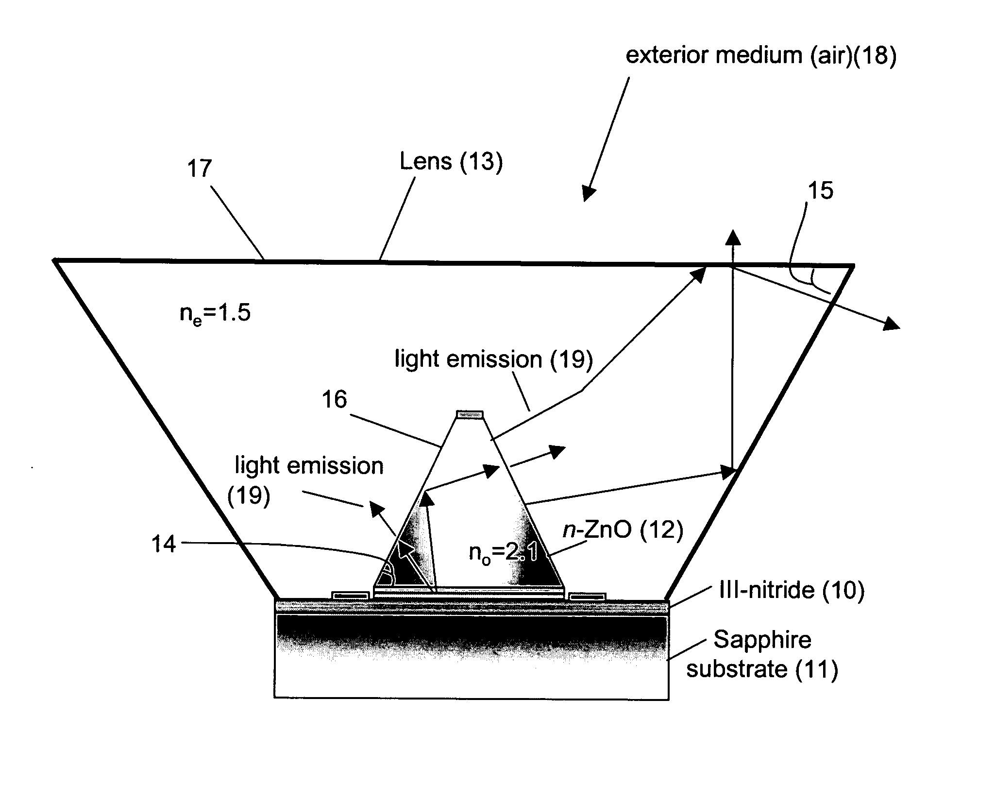
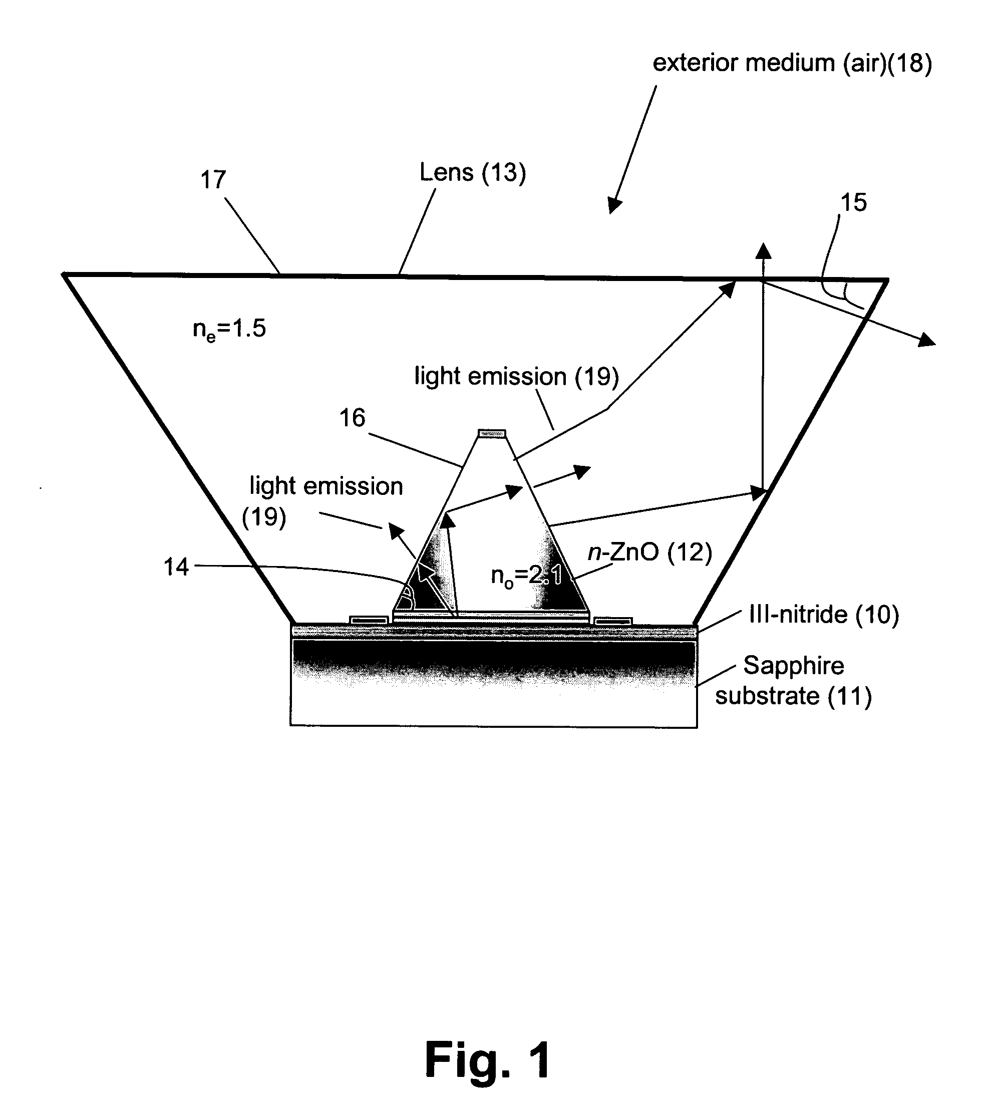
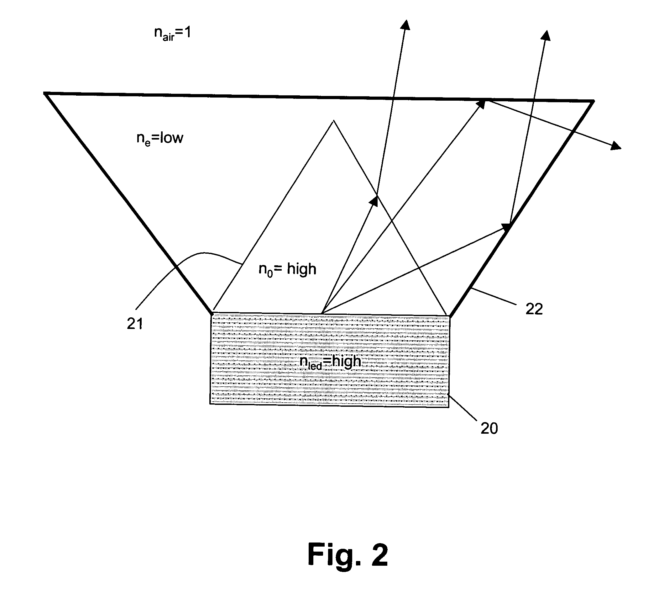
[0056] The present invention describes an (Al, Ga, In)N and ZnO direct wafer bonded light emitting diode (LED), combined with a shaped plastic optical element, in which the directional light entering the shaped plastic optical element from a ZnO cone, or any high refractive index material in contact with the LED surface, is extracted to air. In particular, the (Al, Ga, In)N and ZnO direct wafer-bonded LED structure is combined with a tapered lens, in which most of the light entering the lens lies within the critical angle and is extracted.

[0057] The present invention redu...


PUM


Abstract

An (Al, Ga, In)N and ZnO direct wafer bonded light emitting diode (LED) combined with a shaped plastic optical element, in which the directional light from the ZnO cone, or from any high refractive index material in contact with the LED surface, entering the shaped plastic optical element is extracted to air.

Description

CROSS-REFERENCE TO RELATED APPLICATIONS [0001] This application claims the benefit under 35 U.S.C Section 119(e) of U.S. Provisional Application Ser. No. 60 / 734,040, filed on Nov. 4, 2005, by Steven P. DenBaars, Shuji Nakamura, Hisashi Masui, Natalie N. Fellows, and Akihiko Murai, entitled “HIGH LIGHT EXTRACTION EFFICIENCY LIGHT EMITTING DIODE (LED),” attorneys' docket number 30794.161-US-P1 (2006-271-1); [0002] which application is incorporated by reference herein. [0003] This application is related to the following co-pending and commonly-assigned applications: [0004] U.S. Utility application Ser. No. 10 / 581,940, filed on Jun. 7, 2006, by Tetsuo Fujii, Yan Gao, Evelyn. L. Hu, and Shuji Nakamura, entitled “HIGHLY EFFICIENT GALLIUM NITRIDE BASED LIGHT EMITTING DIODES VIA SURFACE ROUGHENING”, attorney's docket number 30794.108-US-WO (2004-063), which application claims the benefit under 35 U.S.C Section 365(c) of PCT Application Ser. No. US2003 / 03921, filed on Dec. 9, 2003, by Tetsuo...

Claims


Application Information

Patent Timeline
IPC IPC(8): H01L33/00H01L33/20H01L33/26H01L33/58H01L33/60
CPCH01L33/007H01L33/20H01L33/26H01L33/58H01L33/60
Inventor DENBAARS, STEVEN P.NAKAMURA, SHUJIMASUI, HISASHIFELLOWS, NATALIE NICHOLEMURAI, AKIHIKO
Owner RGT UNIV OF CALIFORNIA
Why Eureka
Try Eureka