

Method for pre-treating epitaxial layer, method for evaluating epitaxial layer, and apparatus for evaluating epitaxial layer
a technology of epitaxial layer and epitaxial layer, which is applied in the direction of individual semiconductor device testing, semiconductor/solid-state device testing/measurement, instruments, etc., can solve the problem of delay in measurement feed-back, large amount of solution containing oxidizing agent, and relatively long treatment time of about 20 to 30 minutes, so as to improve evaluation efficiency, reduce dispersion of measured value, and short pretreatment time
- Summary
- Abstract
- Description
- Claims
- Application Information
AI Technical Summary
Benefits of technology
Problems solved by technology
Method used
Image

Examples
example 1
Comparison of Pretreatment Method of the Invention and a Conventional Method
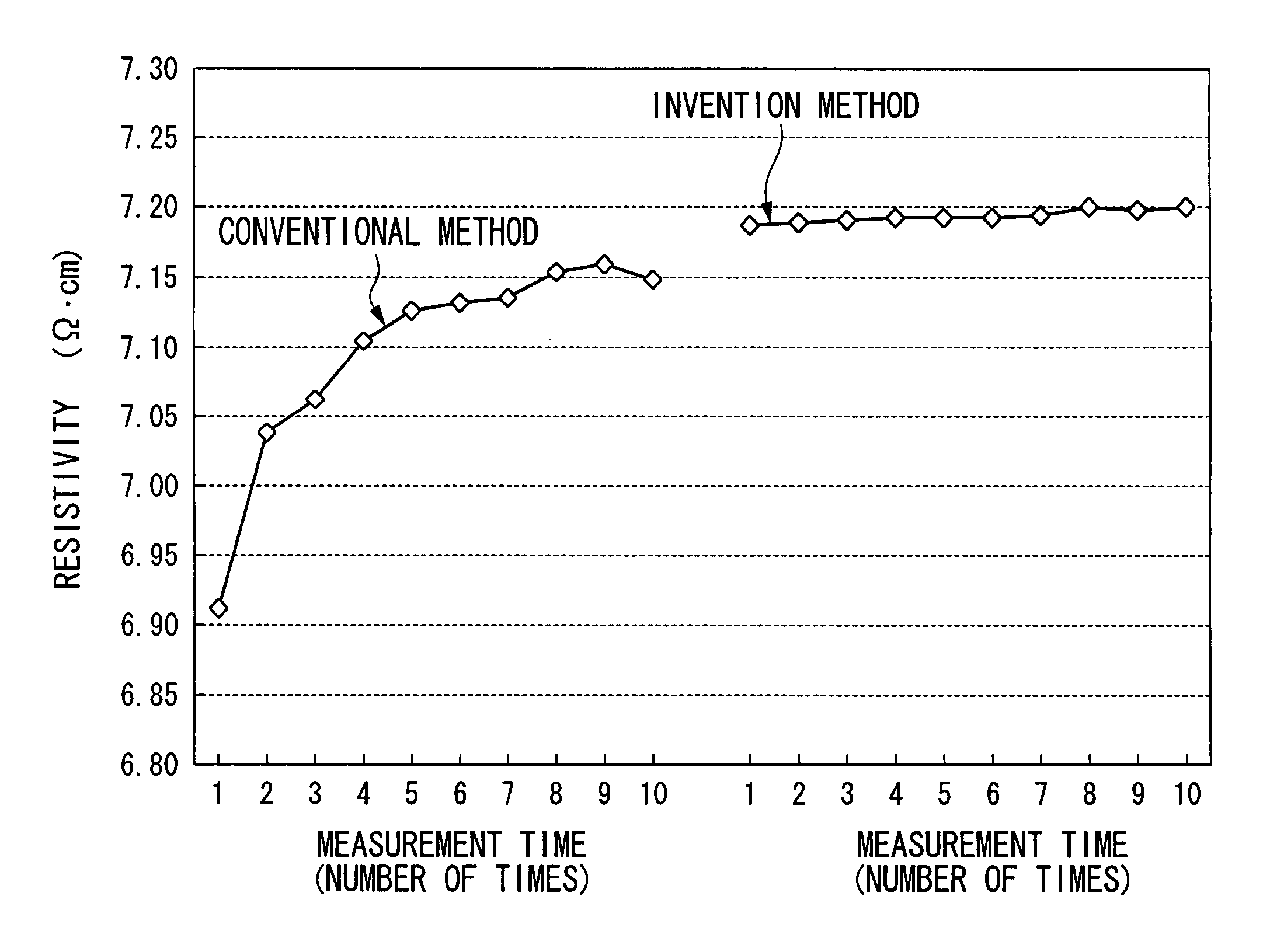
[0091] As Experimental Example 1, the pre-treatment method of the present invention was compared with a conventional method.
[0092] The pretreatment method of the present invention was performed using the following procedure.
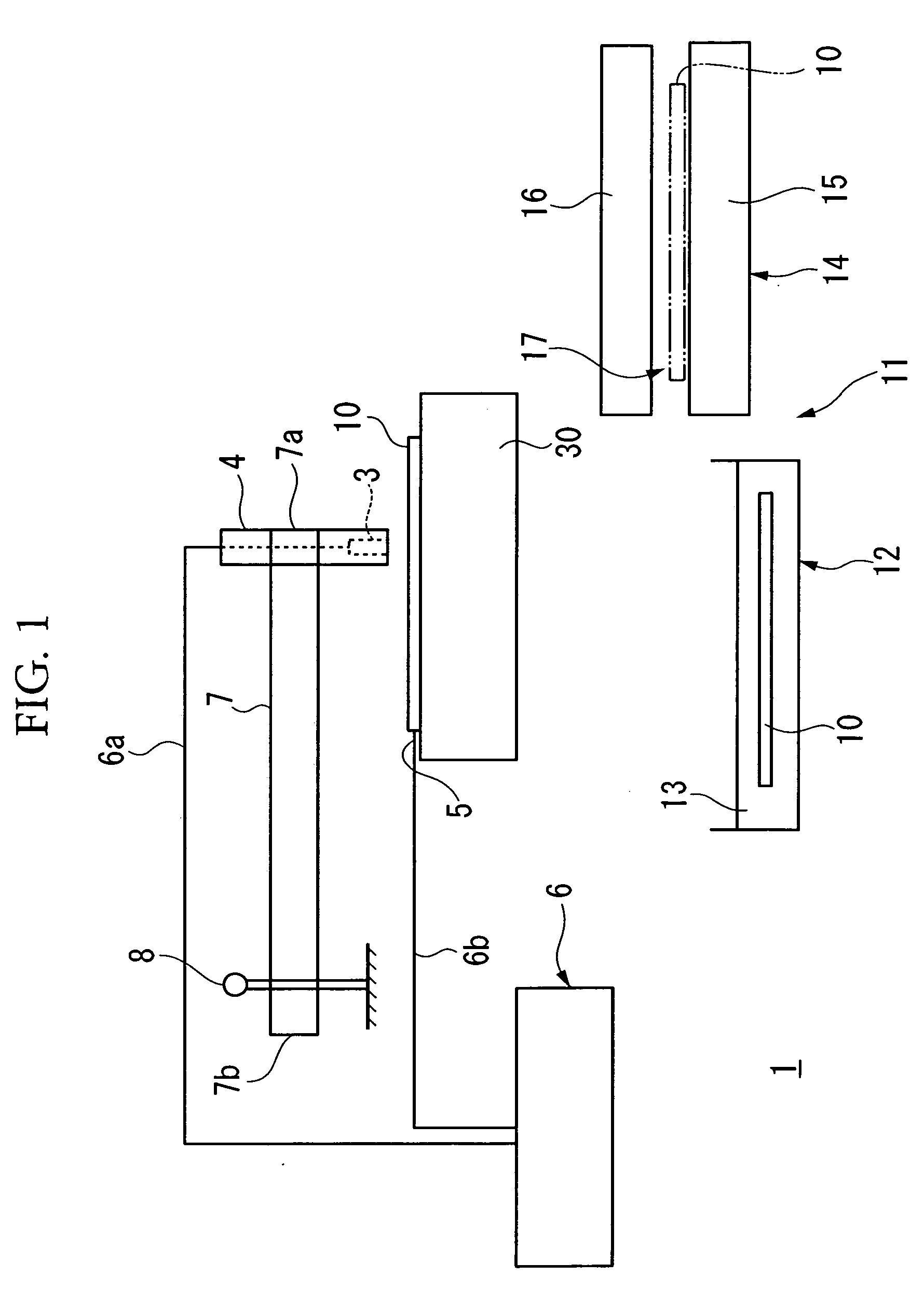
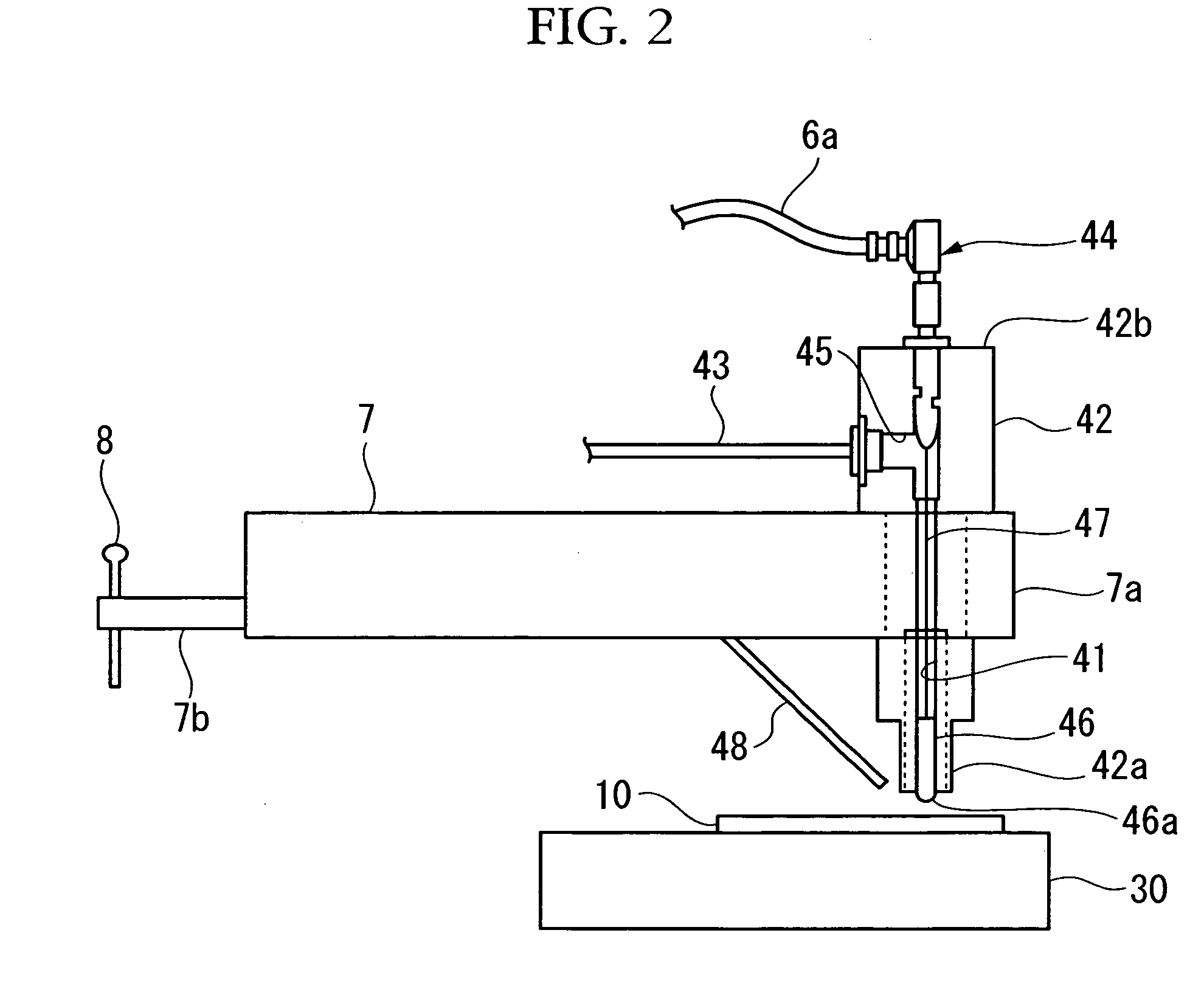
[0093] Firstly, as objects of evaluation, N-type silicon wafers (hereafter referred to as sample wafers 1 were prepared so as to have a n-type epitaxial silicon layer of designed resistivity of 7.2 Ω·cm on an n-type silicon wafer respectively). In addition, in accordance with a constitution schematically shown in FIG. 1, an apparatus for measuring a resistivity was prepared. A reservoir of the apparatus was filled with a diluted solution in which dissolved a carbon-bearing compound, polyoxyethylene-p-(1,1,3,3,-tetramethylbutyl)-phenylether was dissolved. In the diluted solution, stock solution was diluted to 1000 times with water. The stock solution was a mixed solution containing 25 t...
example 2
Evaluation of Reproducibility of the Pretreatment Method of the Present Invention
[0100] As objects of evaluation, three types of epitaxial wafers (hereafter referred to as sample wafers 2, sample wafers 3, and sample wafers 4) were prepared. Sample wafers 2 had an n-type epitaxial layer of designed resistivity of 30.91 Ω·cm layered on a p-type silicon wafer; sample wafers 3 had an n-type epitaxial layer of designed resistivity of 7.205 Ω·cm layered on a n-type silicon wafer; and sample wafers 4 had an n-type epitaxial layer of designed resistivity of 0.354 Ω·cm layered on a n-type silicon wafer. Each of the wafers was pretreated with the above-described method of the present invention and above-described conventional method and an oxide film was formed on an epitaxial layer of each wafer. Next, sample wafers 2, 3, 4 which had been pretreated by the method of the present invention and by the conventional method were subjected to, the same as in Example 1, 10 repeated measurements of...
example 3
Evaluation of Stability of Pretreatment-Method in Accordance with the Present Invention
[0105] As objects of evaluation, three types of epitaxial wafers (hereafter referred to as sample wafers 5, sample wafers 6, and sample wafers 7) were prepared. Sample wafer 5 had an n-type epitaxial layer of designed resistivity of 29.86 Ω·cm layered on a p-type silicon wafer; sample wafers 6 had an n-type epitaxial layer of designed resistivity of 7.20 Ω·cm layered on a n-type silicon wafer; and sample wafers 7 had an n-type epitaxial layer of designed resistivity of 0.2591 Ω·cm layered on an n-type silicon wafer. Each of the wafers was pretreated with the above-described method of the present invention and above-described conventional method and an oxide film was formed on an epitaxial layer of each wafer. Next, sample wafers 5, 6, 7 which have been pretreated by the method of the present invention and by the conventional method were subjected to, as same as Example 1, 10 times repeated measur...
PUM
| Property | Measurement | Unit |
|---|---|---|
| wavelength | aaaaa | aaaaa |
| time | aaaaa | aaaaa |
| wavelength | aaaaa | aaaaa |
Abstract
Description
Claims
Application Information