

Protective film for plasma display panel and method for manufacturing this protective film, and plasma display panel and method for manufacturing thereof
- Summary
- Abstract
- Description
- Claims
- Application Information
AI Technical Summary
Benefits of technology
Problems solved by technology
Method used
Image

Examples
examples
SrO—CaO Concentration
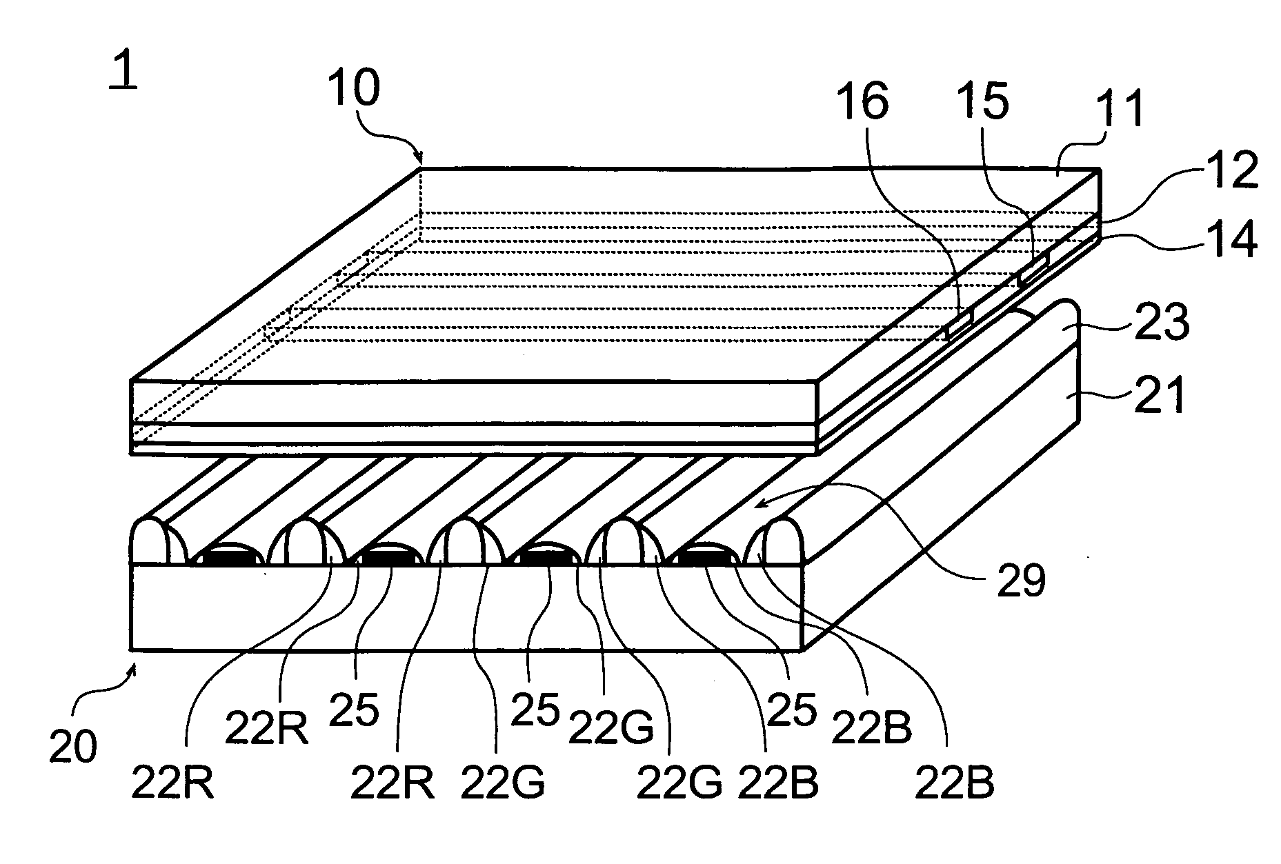
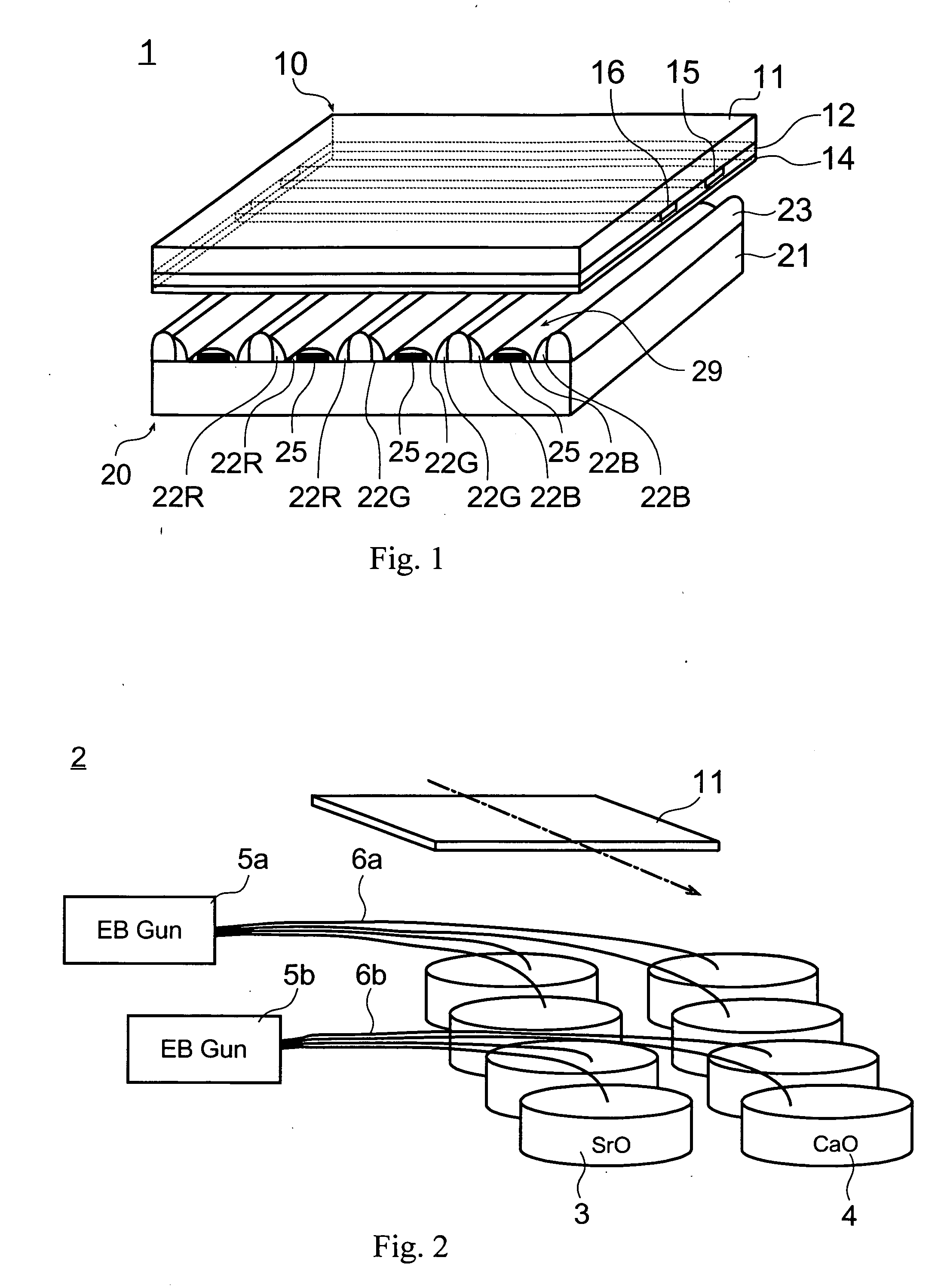
[0070] Plasma display panels 1 having 300 luminescent cells in the surface thereof were obtained by producing protective films 14 of the first and second panels using various concentrations of SrO and CaO. With each plasma display panel 1, the height of the barrier ribs 23 was 150 μm, the height of the space in which discharge occurred (that is, the height from the tops of the fluorescent films 22R, 22G, 22B on the address electrodes 25 to the top of the protective film 14 on the sustaining electrodes 15 and the scanning electrodes 16) was 80 μm; the insert gas was a mixture of neon and xenon (a mixed gas composed of neon and xenon); the xenon concentration of 12 vol %; and the charging pressure of the inert gas was 400 Torr.
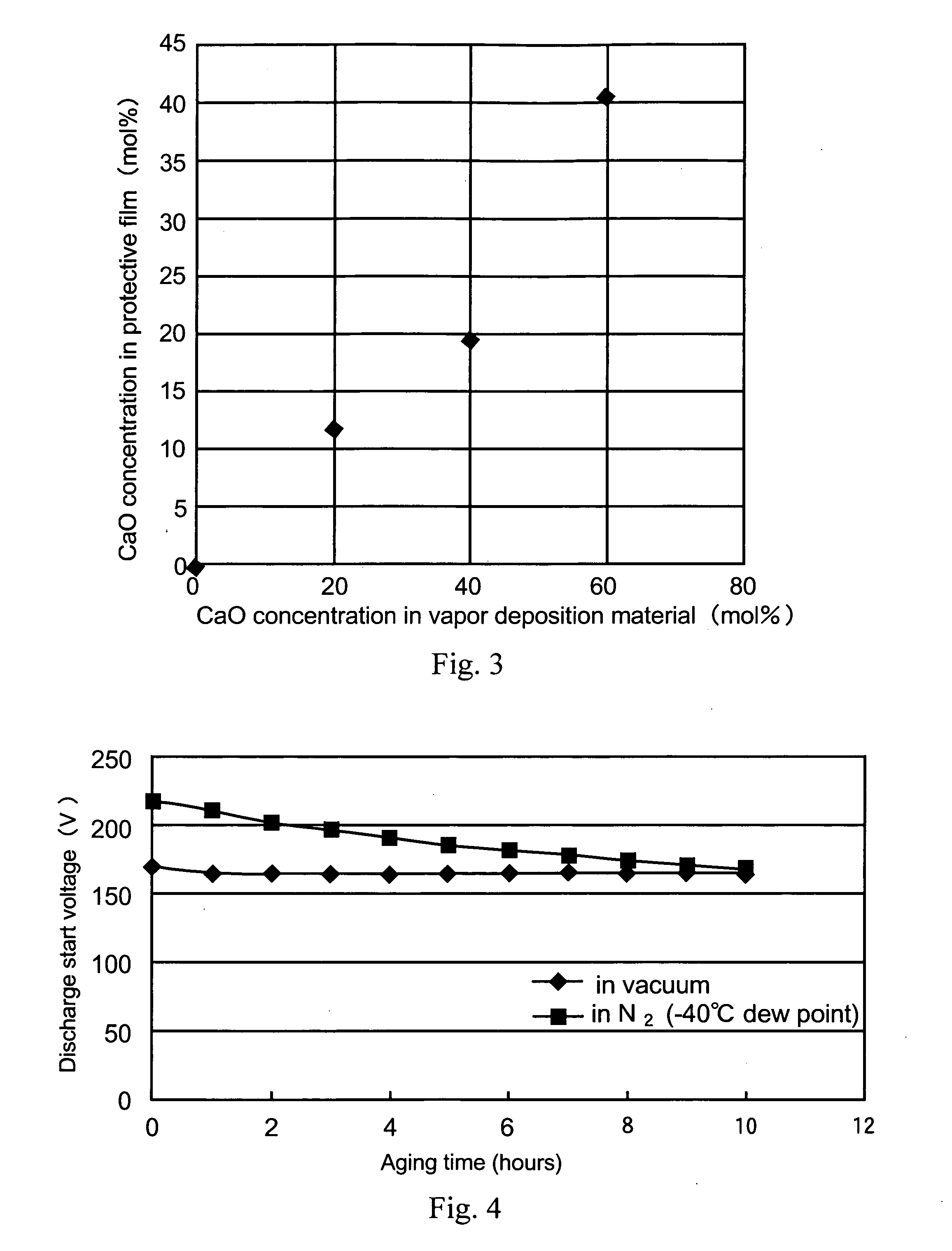
[0071] Table 1 shows the CaO concentration (mol %) in the protective film 14.
[0072] The CaO concentrations (mol %) in the protective film 14 are shown in the following Table 1.
TABLE 1Results of measuring discharge voltage and sputterin...
PUM
| Property | Measurement | Unit |
|---|---|---|
| Fraction | aaaaa | aaaaa |
| Fraction | aaaaa | aaaaa |
| Fraction | aaaaa | aaaaa |
Abstract
Description
Claims
Application Information