Semiconductor device and method for processing wafer
a technology of semiconductor devices and wafers, applied in metal working equipment, manufacturing tools, welding/soldering/cutting articles, etc., can solve the problems of difficult to completely absorb particle particles, large size of semiconductor devices, and low yield ratio, and achieve the effect of improving yield ratio and quality of chips
- Summary
- Abstract
- Description
- Claims
- Application Information
AI Technical Summary
Benefits of technology
Problems solved by technology
Method used
Image

Examples
first embodiment
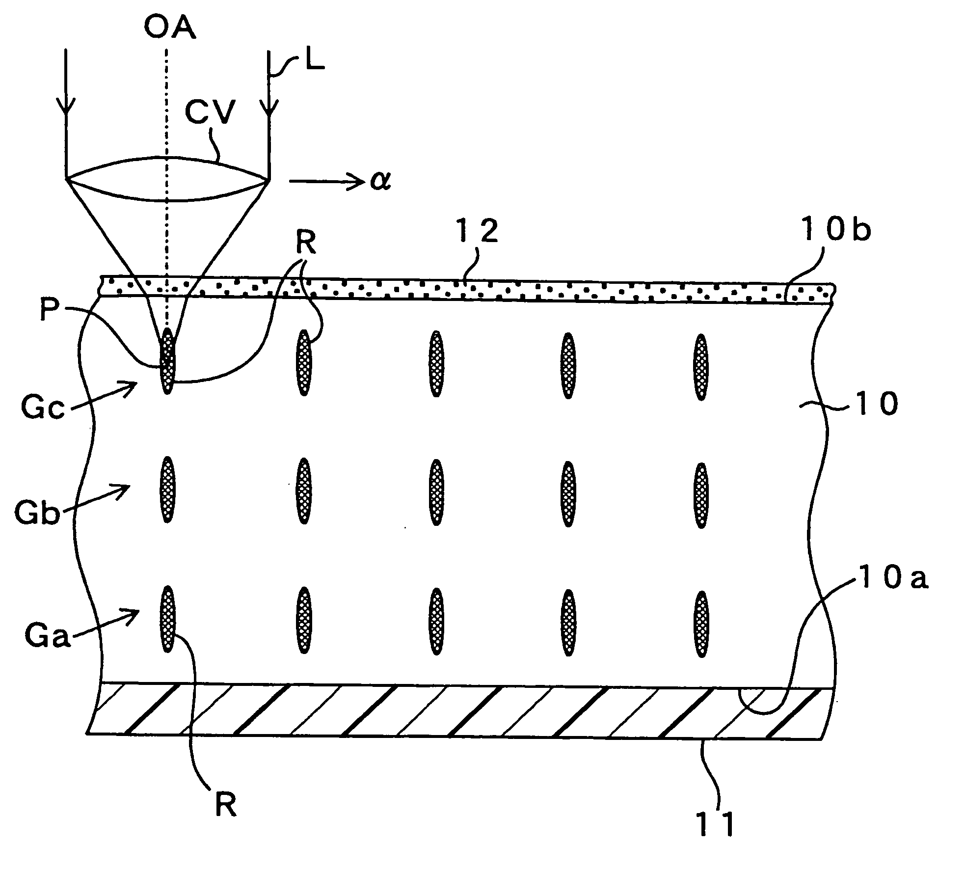
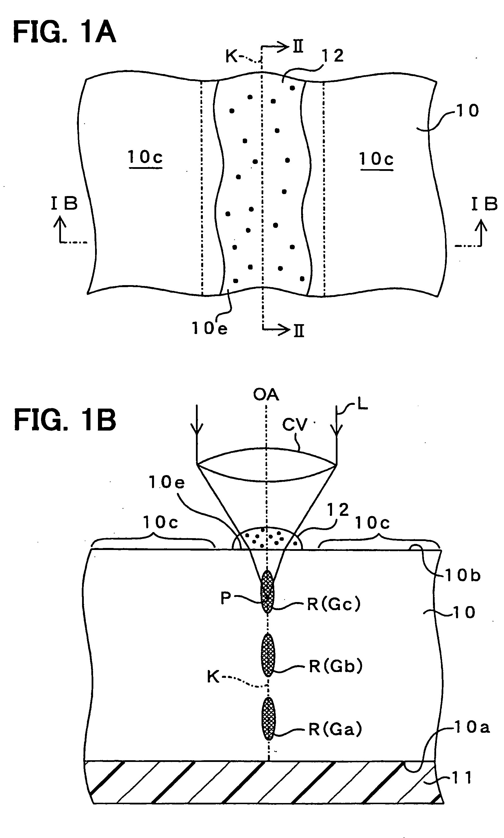
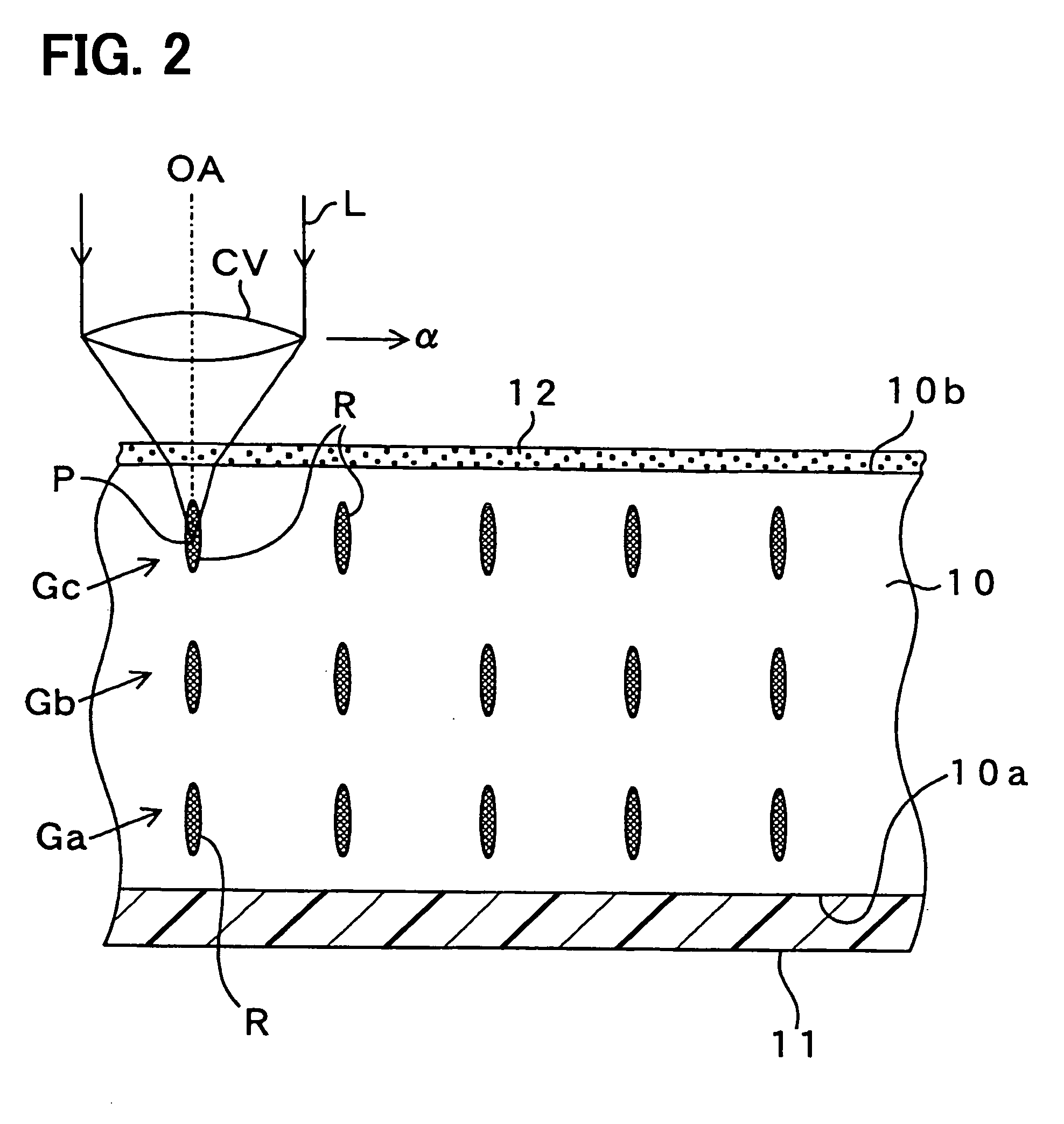
[0053]FIGS. 1A, 1B and 2 show a method for processing a wafer. Specifically, FIGS. 1A, 1B and 2 explain a step of forming a reforming portion by irradiating a laser beam on a wafer 10. The wafer 10 such as a bulk silicon wafer is made from bulk single crystal silicon, and has a backside 10a. A dicing film 11 such as a dicing seat, a dicing tape or an expandable tape is formed on the backside 10a of the wafer 10.
[0054] The dicing film 11 is made from a plastic film. The dicing film 11 is extendable by applying a force in an extendable direction and by heating. The dicing film 11 is adhered on whole area of the backside of the wafer 10 with adhesive (not shown).
[0055] A device forming region 10c is formed on the foreside 10b of the wafer 10. In the device forming region 10c, a semiconductor device (not shown) is formed. The semiconductor device is, for example, a monolithic IC, a semiconductor element, a sensor or a micro-machine. The sensor and the micro-machine are formed by a MEM...
second embodiment
[0114]FIGS. 4A and 4B show a method for processing the wafer 10. Specifically, FIGS. 4A and 4B show another method for forming the reforming portions R in the wafer 10. The wafer 10 includes a concavity 21 on the surface 10b of the wafer 10. The concavity 21 is disposed on the part 10e of the wafer 10, and has a U-shaped cross section with a corner. The thermoplastic member 12 is formed in the concavity 21.
[0115] When the wafer 10 is cut and separated from the cutting line K, and the melted thermoplastic member 12 falls along with the dicing surface 10d, since the thermoplastic member 12 is accommodated in the concavity 21, the melted thermoplastic member 12 does not extend on the device forming region 10c. Specifically, the melted thermoplastic member 12 does not overflow from the concavity 21, and therefore, the thermoplastic member 12 does not reach the device forming region 10c on the surface 10b of the wafer 10. Thus, all melted thermoplastic member 12 falls down into the dici...
third embodiment
[0120]FIGS. 6A and 6B show a method for processing the wafer 10. Specifically, FIGS. 6A and 6B show further another method for forming the reforming portions R in the wafer 10.
[0121] The wafer 10 includes a pair of concavities 31a, 31b on the surface 10b of the wafer 10. Each concavity 31a, 31b are disposed between the cutting line K and the device forming region 10c, and has a U-shaped cross section with a corner. Thus, the concavities 31a, 31b are disposed in parallel to the cutting line K so that the cutting line K is sandwiched between the concavities 31a, 31b. Firstly, the thermoplastic member 12 is formed on the part 10e of the wafer 10.
[0122] When the wafer 10 is cut and separated from the cutting line K, and the melted thermoplastic member 12 falls along with the dicing surface 10d, since the concavities 31a, 31b are disposed between the part 10e of the wafer 10 and the device forming region 10c, the melted thermoplastic member 12 does not extend on the device forming regi...
PUM
| Property | Measurement | Unit |
|---|---|---|
| Pressure | aaaaa | aaaaa |
| Shrinkage | aaaaa | aaaaa |
| Structure | aaaaa | aaaaa |
Abstract
Description
Claims
Application Information
 - Generate Ideas
- Intellectual Property
- Life Sciences
- Materials
- Tech Scout
- Unparalleled Data Quality
- Higher Quality Content
- 60% Fewer Hallucinations
Browse by: Latest US Patents, China's latest patents, Technical Efficacy Thesaurus, Application Domain, Technology Topic, Popular Technical Reports.
© 2025 PatSnap. All rights reserved.Legal|Privacy policy|Modern Slavery Act Transparency Statement|Sitemap|About US| Contact US: help@patsnap.com