SiC EPITAXIAL WAFER AND METHOD FOR PRODUCING SAME
a technology of epitaxial wafers and epitaxial wafers, which is applied in the direction of crystal growth process, polycrystalline material growth, chemically reactive gas growth, etc., can solve the problems of increasing the yield ratio of crystal defects such as triangular defects, device killer defects, and difficult to obtain the same, so as to achieve the effect of high device yield
- Summary
- Abstract
- Description
- Claims
- Application Information
AI Technical Summary
Benefits of technology
Problems solved by technology
Method used
Image


Examples
examples
[0132]Hereinafter, examples of the present invention will be described. However, the present invention is not limited thereto.
Examination of Basal Plane Dislocation
examples 1-1 to 1-5
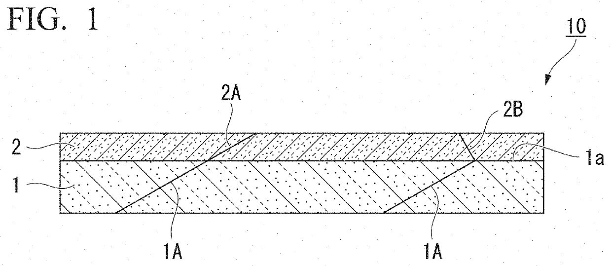
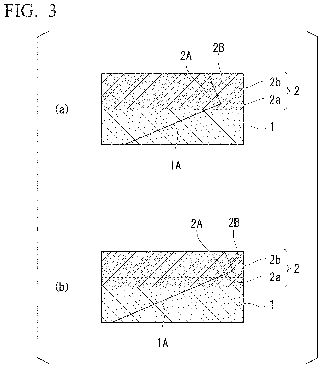
[0133]A SiC single crystal substrate having a size of 4 inches was prepared. The prepared SiC single crystal substrate was a 4H polytype, and a main surface had an off-angle of 4°.
[0134]Next, the SiC single crystal substrate was introduced into a growth furnace, and gas etching was performed on a growth surface using hydrogen gas. The etching temperature was set to a temperature the same as the epitaxial growth temperature.
[0135]Next, an epitaxial layer was grown on a surface of the etched 4H-SiC single crystal substrate while supplying silane and propane as raw material gas, and hydrogen as carrier gas. A first growth rate VA in a first step was set to 4 μm / h, and a second growth rate VB was set to 75 μm / h. The maximum increase rate of the growth rate from the first growth rate VA to the second growth rate VB in the first step was set to 0.4 μm / (h·sec).
[0136]The maximum increase rate of the growth rate was obtained using a calculation method as follows. The flow rate of silicon-bas...
example 2-1
[0139]Example 2-1 is different from Example 1-1 in that the second growth rate VB was set to 60 μm / h. The other conditions were the same as those in Example 1-1. A basal plane dislocation density of a SiC epitaxial wafer obtained in Example 2-1 was also evaluated. The obtained results are shown in Table 1 and FIG. 6.
PUM
| Property | Measurement | Unit |
|---|---|---|
| off-angle | aaaaa | aaaaa |
| diameter | aaaaa | aaaaa |
| thickness | aaaaa | aaaaa |
Abstract
Description
Claims
Application Information
 - Generate Ideas
- Intellectual Property
- Life Sciences
- Materials
- Tech Scout
- Unparalleled Data Quality
- Higher Quality Content
- 60% Fewer Hallucinations
Browse by: Latest US Patents, China's latest patents, Technical Efficacy Thesaurus, Application Domain, Technology Topic, Popular Technical Reports.
© 2025 PatSnap. All rights reserved.Legal|Privacy policy|Modern Slavery Act Transparency Statement|Sitemap|About US| Contact US: help@patsnap.com