

Wafer product and processing method therefor
a technology of wafers and products, applied in the field of wafer products, can solve the problems of damage to the expansible sheet attached to the rear face of the wafer, the inability to position the focal point of the inability to position the laser light inside the wafer
- Summary
- Abstract
- Description
- Claims
- Application Information
AI Technical Summary
Benefits of technology
Problems solved by technology
Method used
Image

Examples
first embodiment
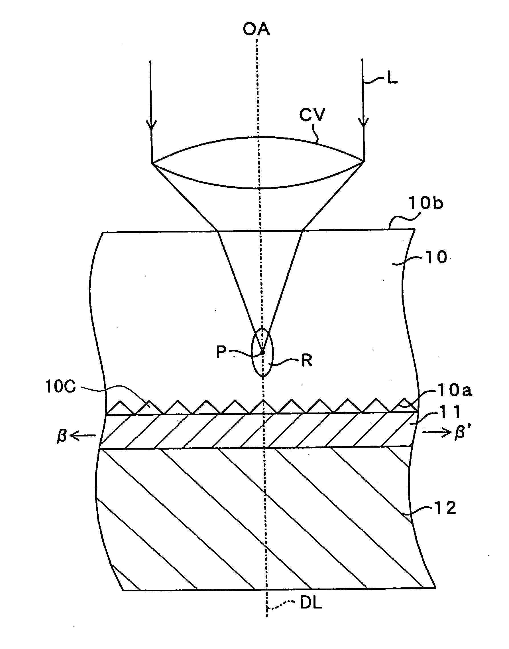
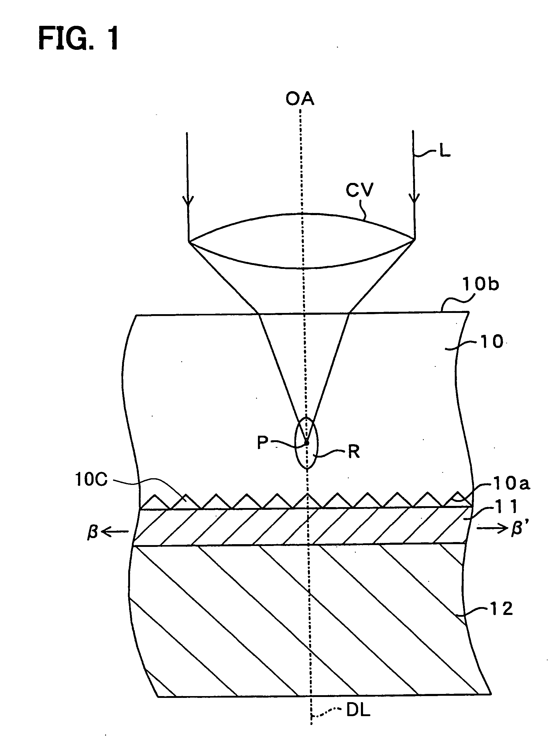
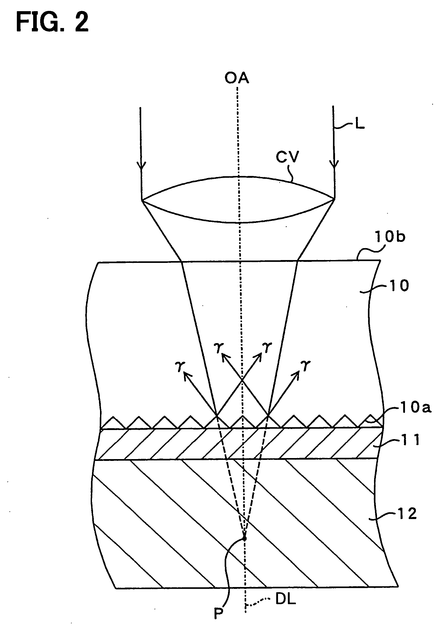
[0044] Referring first to FIGS. 1 and 2, a bulk silicon wafer 10 is formed of a bulk material of single crystal silicon, and its rear face 10a is a roughened surface in which substantially uniform projections and depressions 10c are formed as a protection layer. To make the rear face 10a of the wafer 10 a roughened surface, that is, protection layer, any processing method may be used. Examples of the processing method include: a method in which the rear face 10a is immersed in acid solution or alkaline solution that affects the material for forming the wafer 10 and chemically treated; and a method in which the rear face is processed by mechanical polishing, such as sandblast.
[0045] To cut and separate the wafer 10 using a laser dicing technology, the following procedure is taken: a dicing sheet (dicing film, dicing tape, expand tape) 11 is stuck to the rear face 10a of the wafer 10. The dicing sheet 11 is composed of expansible plastic sheet material that is stretched by applying h...
second embodiment
[0078] The second embodiment shown in FIG. 8 is different from the first embodiment in the following points.
[0079] (2.1) The rear face 10a of the wafer 10 is a smooth surface.
[0080] (2.2) The dicing sheet 11 is composed of a sheet base material 11a and a binding material 11b, and the binding material 11b is applied to the entire front face of the sheet base material 11a.
[0081] (2.3) The sheet base material 11a is formed of an expansible plastic sheet material, and its front face is a smooth surface. The binding material 11b is formed of a thin sheet of adhesive having the property of bonding together the wafer 10 and the sheet base material 11a. An example of this adhesive is acrylic adhesive. The front face of the binding material 11b is a roughened surface in which substantially uniform projections and depressions are formed, so that the binding material functions as a protection layer for protecting the base material 11a from the laser light L.
[0082] (2.4) The rear face 10a o...
third embodiment
[0087] In the third embodiment shown in FIG. 9, the rear face 10a of the wafer 10 is a smooth surface and the dicing sheet 11 is formed of the sheet base material 11a and the binding material 11b as described in Sections 2.1 and 2.2 with regard to the second embodiment.
[0088] The third embodiment is different from the second embodiment only in the following:
[0089] (3.1) The front face of the sheet base material 11a is a roughened surface in which substantially uniform projections and depressions are formed. The front face of the binding material 11b is a smooth surface.
[0090] (3.2) The entire rear face 10a of the wafer 10 is stuck to the front face of the binding material 11b. The front face (in contact with the binding material 11b) of the sheet base material 11a is a roughened surface.
[0091] Therefore, even when a light-converging point P is erroneously set to a point beyond the rear face 10a of the wafer 10, the above problem does not arise. Since the laser light L is scatter...
PUM
| Property | Measurement | Unit |
|---|---|---|
| surface roughness | aaaaa | aaaaa |
| wavelength | aaaaa | aaaaa |
| light scattering | aaaaa | aaaaa |
Abstract
Description
Claims
Application Information