OPC conflict identification and edge priority system

a conflict identification and edge priority technology, applied in the field of integrated circuit verification systems, can solve the problems of reducing the performance of the resulting ic, the fringing effect of the illumination light producing errors on the wafer, and the difficulty in accurately forming features with the photolithographic process, so as to achieve better opc results and better opc correction

Active Publication Date: 2007-05-24
SIEMENS PROD LIFECYCLE MANAGEMENT SOFTWARE INC
View PDF82 Cites 40 Cited by
  • Summary
  • Abstract
  • Description
  • Claims
  • Application Information

AI Technical Summary

Benefits of technology

[0007] The present invention is a tool for alerting a user to conflicts between an optical and process correction (OPC) tool and other system constraints that are preventing a better OPC correction from being made for a feature in an IC layout. Such system constraints are typically user-defined or are process dependent. Upon receiving the alert, the user may be able to change the layout or relax or suspend the system constraint in order to achieve a better OPC result.

Problems solved by technology

As the density of features to be created in an integrated circuit (IC) increases and the size of individual features decrease, such features are increasingly more difficult to accurately form with a photolithographic process.
It is a well documented phenomenon in photolithographic processing that as a feature size becomes smaller than the wavelength of the light that is used to illuminate a mask or reticle pattern onto a wafer, the fringing effects of the illumination light produce errors on the wafer.
Such errors distort the patterns created on a wafer in a manner that may decrease the performance of the resulting IC or cause it to fail completely.
Even when using an OPC tool, some features in an IC design may not print as desired on a wafer.
In many instances, a less than desired OPC correction is made by the OPC tool due to manufacturing constraints that can affect the OPC tool in a non-intuitive manner.
A process of manual debugging takes time, increases the cost and decreases the throughput of overall circuit design process.

Method used


Image

  • OPC conflict identification and edge priority system
  • OPC conflict identification and edge priority system
  • OPC conflict identification and edge priority system

Examples


Embodiment Construction

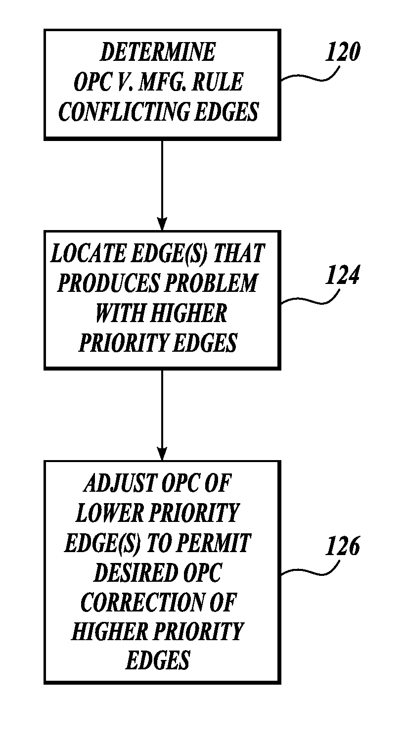
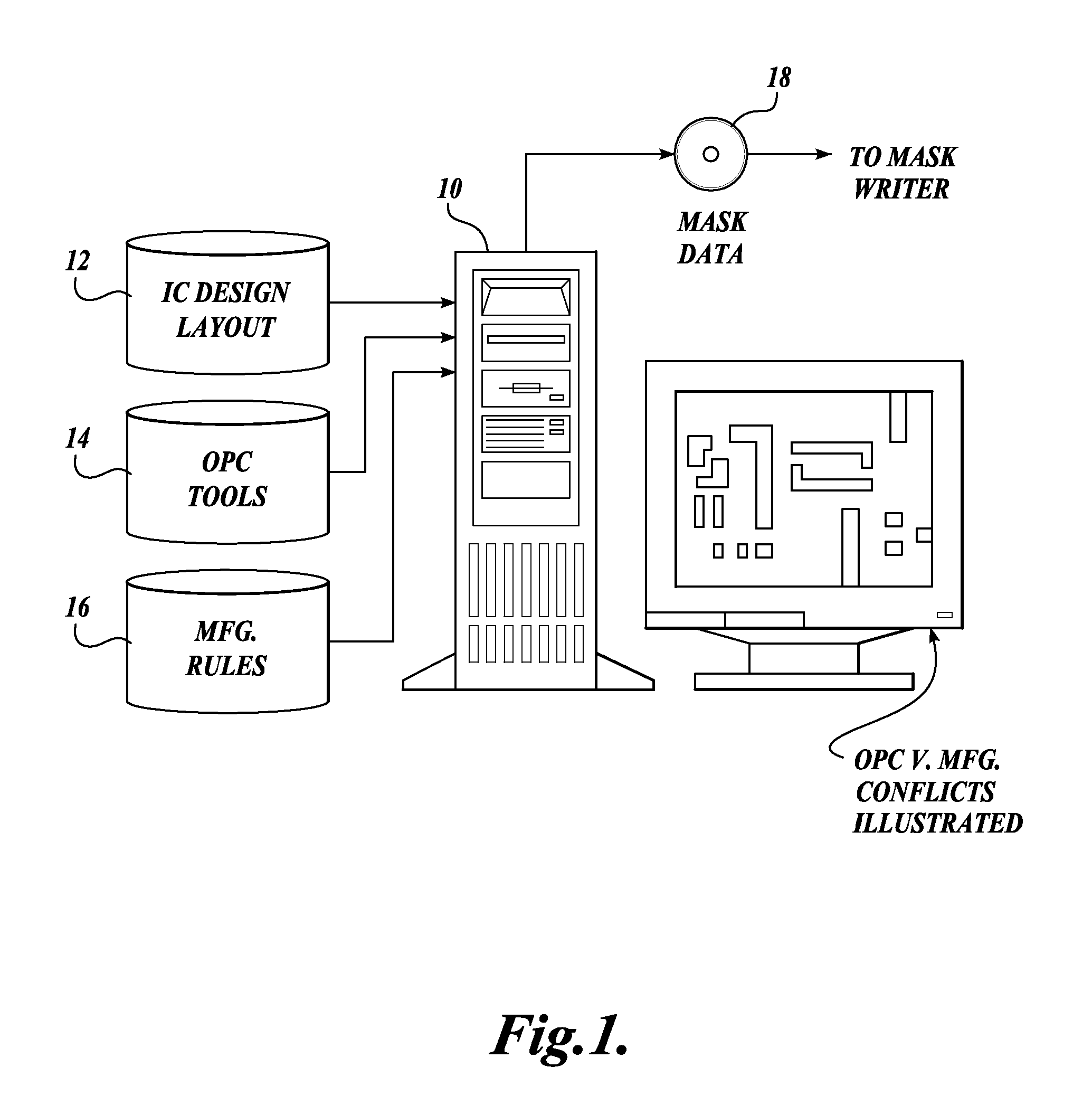
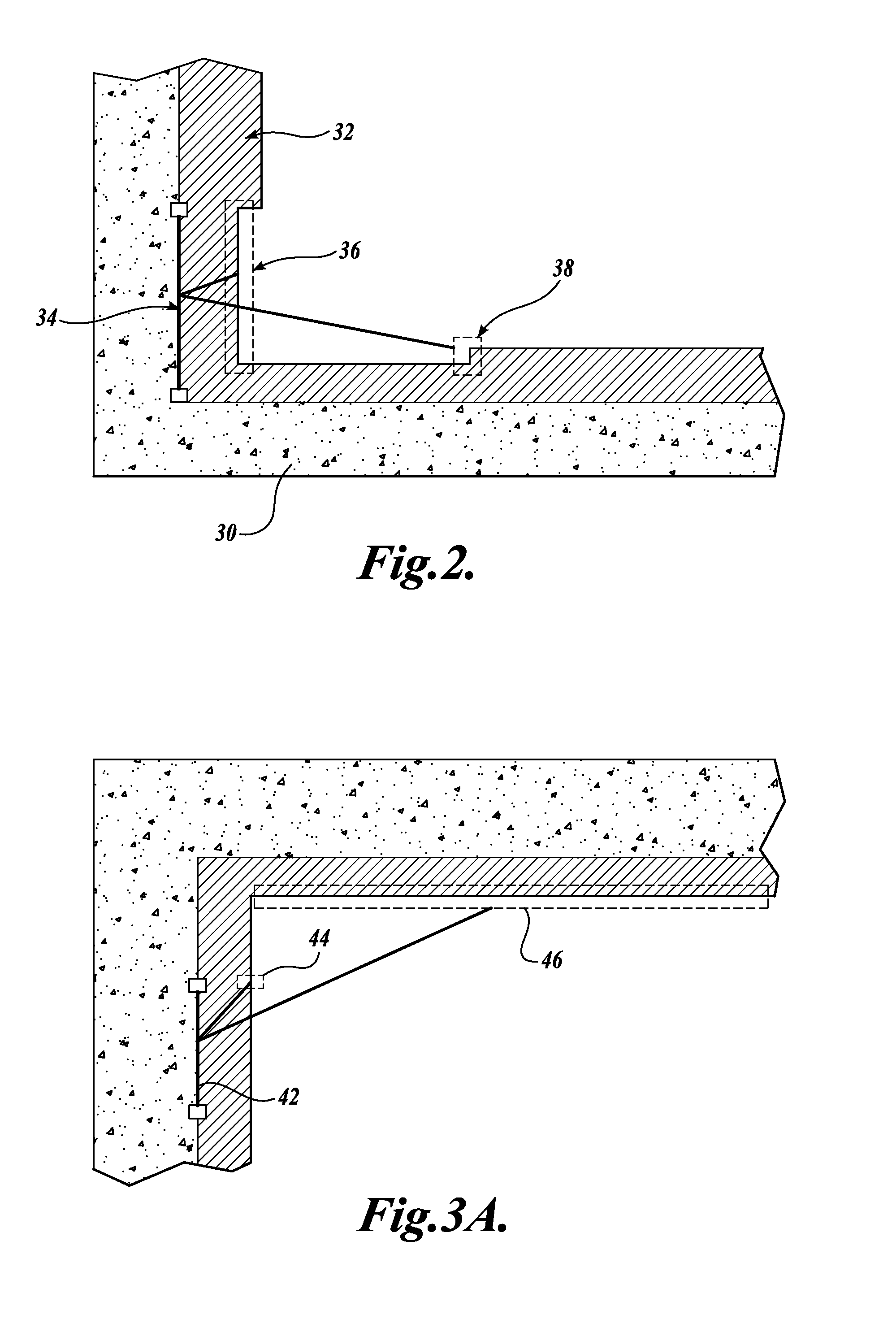
[0016] As indicated above, one aspect of the present invention is a system for performing IC layout data verification that alerts a circuit designer where an optical and process correction (OPC) tool may produce a less than optimal result due to a conflict with other system constraints. As shown in FIG. 1, the layout verification system includes a computer system 10 that receives data from a file 12 containing an IC layout design. The IC layout data may be in a standard layout language such as GDS II, OASIS, or other known formats for describing an IC layout design. In a GDS II layout file, each feature to be created on a wafer is described as a number of vertices that define a polygon outlining the shape of the feature or other structure such as a phase shifter, assist bar, etc., to be created in the circuit. The computer system 10 verifies the layout design with the use of a number of software tools including an OPC tool 14. The OPC tool 14 attempts to modify the edges of the poly...


PUM

PropertyMeasurementUnit
densityaaaaaaaaaa
sizeaaaaaaaaaa
wavelengthaaaaaaaaaa

Abstract

An integrated circuit verification system provides an indication of conflicts between an OPC suggested correction and a manufacturing rule. The indication specifies which edge segments are in conflict so that a user may remove the conflict to achieve a better OPC result. In another embodiment of the invention, edge segments are assigned a priority such that the correction of a lower priority edge does not hinder a desired OPC correction of a higher priority edge.

Description

CROSS-REFERENCE TO RELATED APPLICATION [0001] This application is a divisional of U.S. patent application Ser. No. 10 / 859,920, filed Jun. 2, 2004.FIELD OF THE INVENTION [0002] The present invention relates to integrated circuit verification systems, and in particular, to optical and process correction (OPC) tools. BACKGROUND OF THE INVENTION [0003] As the density of features to be created in an integrated circuit (IC) increases and the size of individual features decrease, such features are increasingly more difficult to accurately form with a photolithographic process. It is a well documented phenomenon in photolithographic processing that as a feature size becomes smaller than the wavelength of the light that is used to illuminate a mask or reticle pattern onto a wafer, the fringing effects of the illumination light produce errors on the wafer. Such errors distort the patterns created on a wafer in a manner that may decrease the performance of the resulting IC or cause it to fail ...

Claims


Application Information

Patent Timeline
Patent Type & Authority Applications(United States)
IPC IPC(8): G06F17/50G03F1/14G06F9/45
CPCG03F1/144G03F1/36
Inventor LIPPINCOTT, GEORGE P.
Owner SIEMENS PROD LIFECYCLE MANAGEMENT SOFTWARE INC
Why Eureka
Try Eureka