

High-Power Pulsed Magnetron Sputtering
a pulsed magnetron and sputtering technology, applied in the direction of electrolysis components, vacuum evaporation coatings, coatings, etc., can solve the problems of relatively low uniformity of films, relatively complex and expensive systems to implement, and the target utilization rate of conventional magnetron sputtering systems is also relatively poor
- Summary
- Abstract
- Description
- Claims
- Application Information
AI Technical Summary
Benefits of technology
Problems solved by technology
Method used
Image

Examples
Embodiment Construction
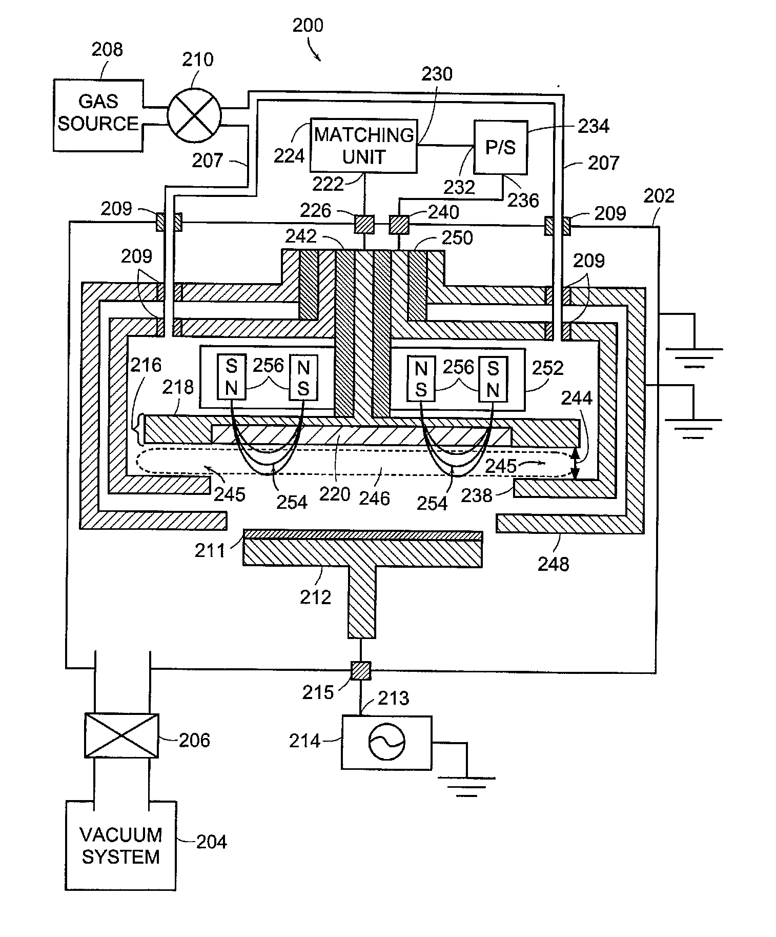
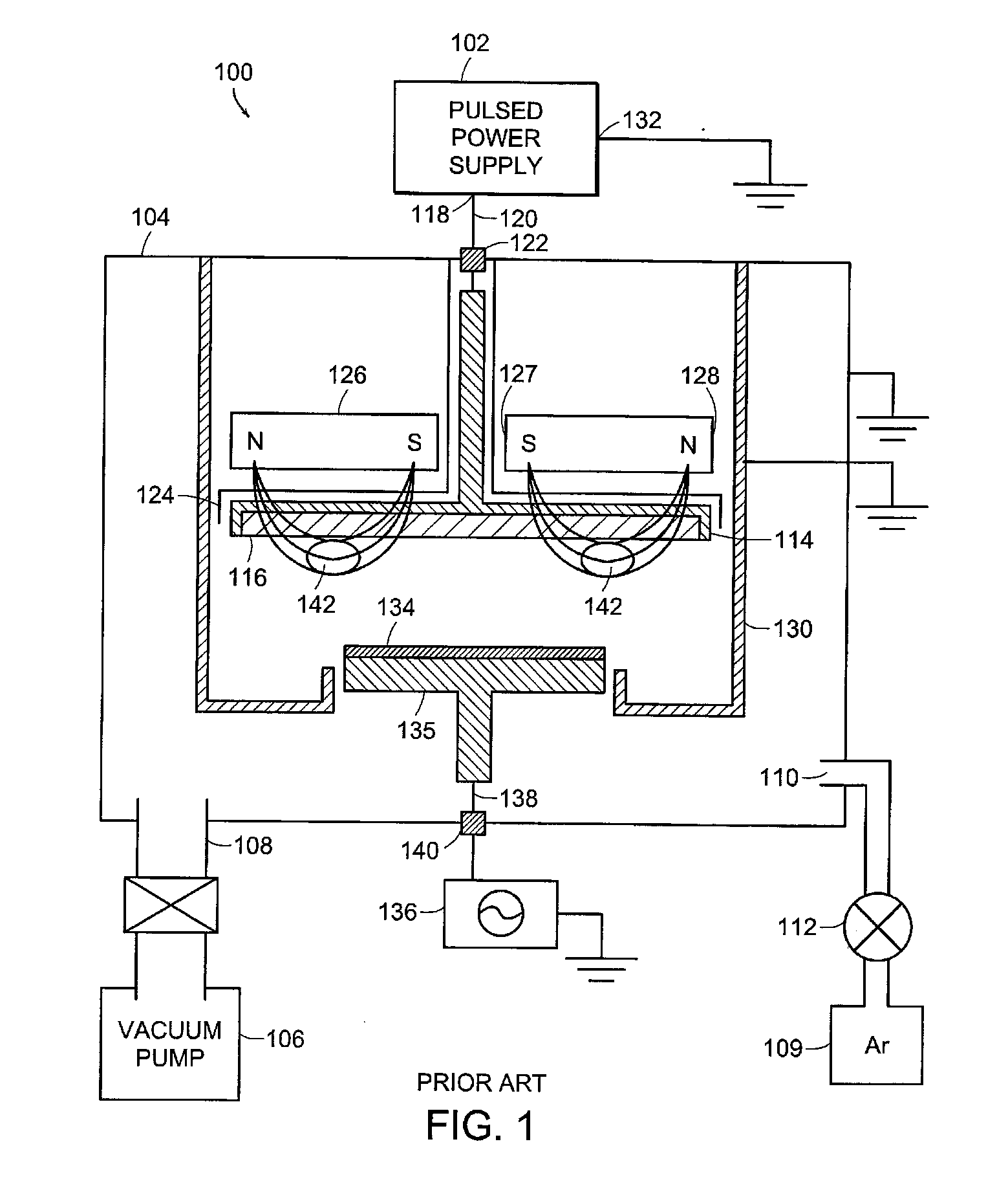
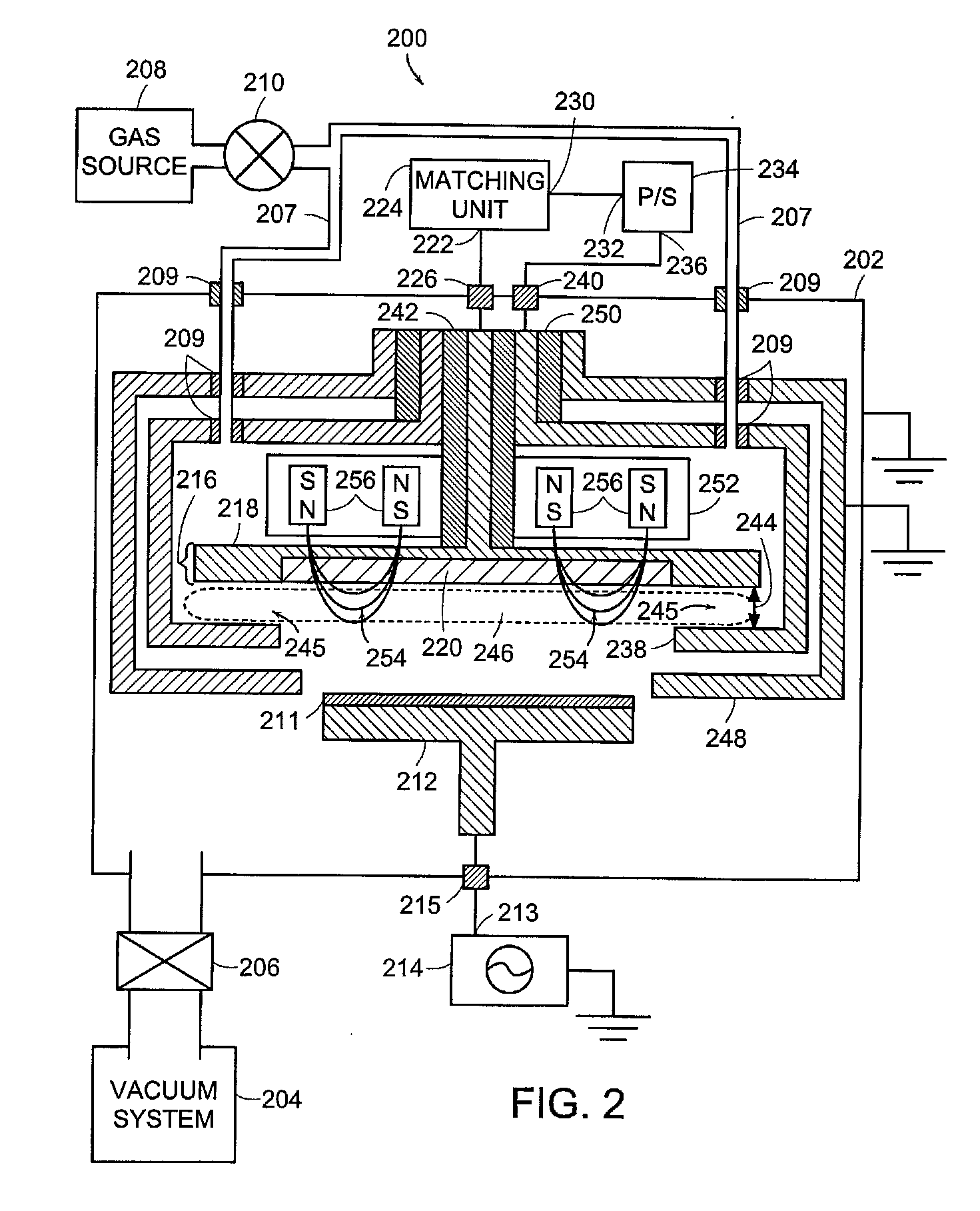
[0021] The magnetic and electric fields in magnetron sputtering systems are concentrated in narrow regions close to the surface of the target. These narrow regions are located between the poles of the magnets used for producing the magnetic field. Most of the ionization of the sputtering gas occurs in these localized regions. The location of the ionization regions causes a non-uniform erosion or wear of the target that results in poor target utilization.
[0022] Increasing the power applied between the target and the anode can increase the amount of ionized gas and, therefore, increase the target utilization. However, undesirable target heating and target damage can occur. Furthermore, increasing the voltage applied between the target and the anode increases the probability of establishing an undesirable electrical discharge (an electrical arc) in the process chamber.
[0023] Pulsing the power applied to the plasma can be advantageous since the average discharge power can remain low w...
PUM
| Property | Measurement | Unit |
|---|---|---|
| pressures | aaaaa | aaaaa |
| pressures | aaaaa | aaaaa |
| pressure | aaaaa | aaaaa |
Abstract
Description
Claims
Application Information