Phase change material and non-volatile memory device using the same

a phase change material and non-volatile memory technology, applied in the direction of bulk negative resistance effect devices, semiconductor devices, electrical equipment, etc., can solve the problems of stability problems, slow writing speed, disadvantages of sb-te based alloys, etc., and achieve the effect of smaller diatomic bond strength and higher atomic number

Active Publication Date: 2007-05-31
SK HYNIX INC
View PDF1 Cites 85 Cited by
  • Summary
  • Abstract
  • Description
  • Claims
  • Application Information

AI Technical Summary

Benefits of technology

[0012] In accordance with the present invention, there is provided a non-volatile phase change memory cell comprising a compound having the formula (GeASbBTeC)1−X(RaSbTeC)X, wherein Ge is germanium; Sb is antimony; Te is tellurium; R is an element selected from the elements belonging to the IVB group in the periodic table; S is an element selected from the elements belonging to the VB group in the periodic table; A, B, C, a, b and c are atomic mole ratios; x is a mole fraction in the range of 0 to 1; RaSbTeC has same crystal structure as GeASbBTeC; and at least one element of R and S has a higher atomic number and thus a smaller diatomic bond strength than that of the corresponding element in the GeSb portion of Ge—Sb—Te.

Problems solved by technology

Despite its merits as nonvolatile phase change memory material, however, a Ge—Sb—Te based alloy is disadvantageous as it tends to yield slow writing speed.
In addition, there is a stability problem associated with thermal interference between adjacent memory cells.
With density of PCRAM growing higher, binary data stored in amorphous memory cells may be corrupted with ease by unintended crystallization as a result of the heat generated in an adjoining memory cell which undergoes melting during a reset process thereof.
However, the addition of impurities may slow the crystallization process (B. J. Kuh et al, EPCOS 2005).
Further, integrating the memory device by sizing down the cell area is inherently bound by the limits of photolithographic techniques.
However, it is extremely hard to control the dispersion between these two states.

Method used


Image

  • Phase change material and non-volatile memory device using the same
  • Phase change material and non-volatile memory device using the same
  • Phase change material and non-volatile memory device using the same

Examples


example 1

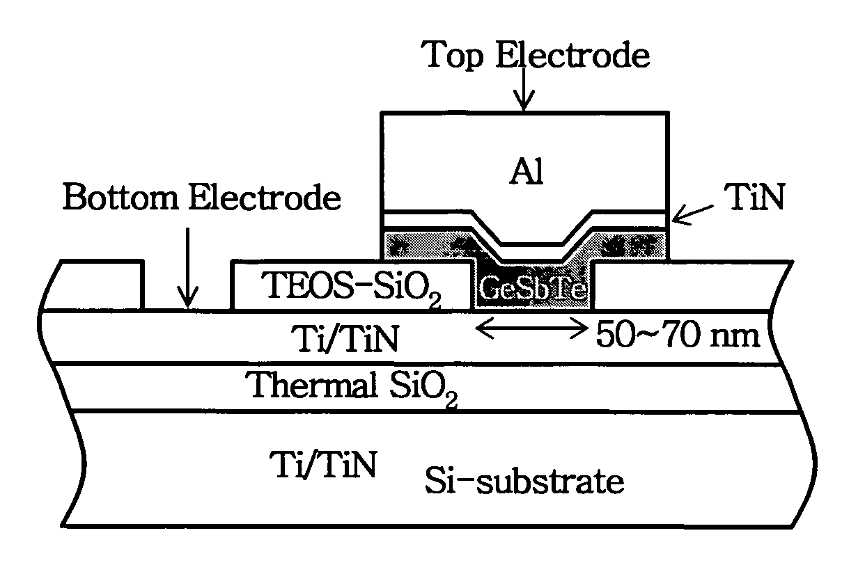
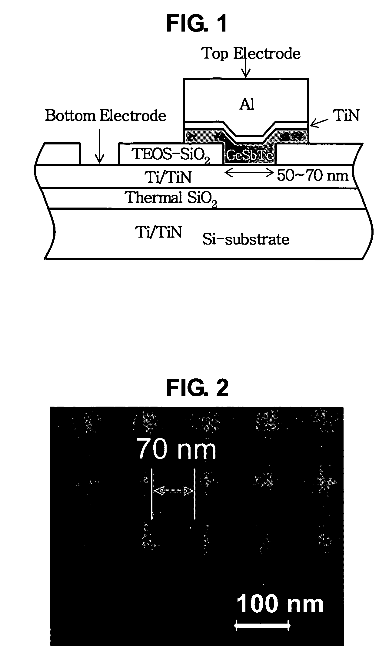
[0037] An off-set type phase change memory cell as shown in FIG. 1 was prepared according to the following procedures. 200 nm-thick SiO2 film was deposited on silicon substrate. Ti / TiN film, as a bottom electrode, was deposited thereon at a thickness of 100 nm, respectively. Next, 100 nm-thick SiO2 was formed thereon. As shown in SEM picture of FIG. 2, a contact hole of 70 nm was formed by electron beam lithography.

[0038] Next, as a phase change material, solid solution of (Ge1Sb2Te4)0.8(Sn1Bi2Te4)0.2 was deposited in the contact hole by PVD (physical vapor deposition) at a thickness of 100 nm. As top electrodes, 100 nm-thick TiN and 500 nm-thick Al films were sequentially deposited on the phase change material.

[0039]FIG. 1 describes a schematic diagram of an off-set type phase change memory cell including a material in accordance with the present invention. Transistor part for cell addressing is not shown in FIG. 1.

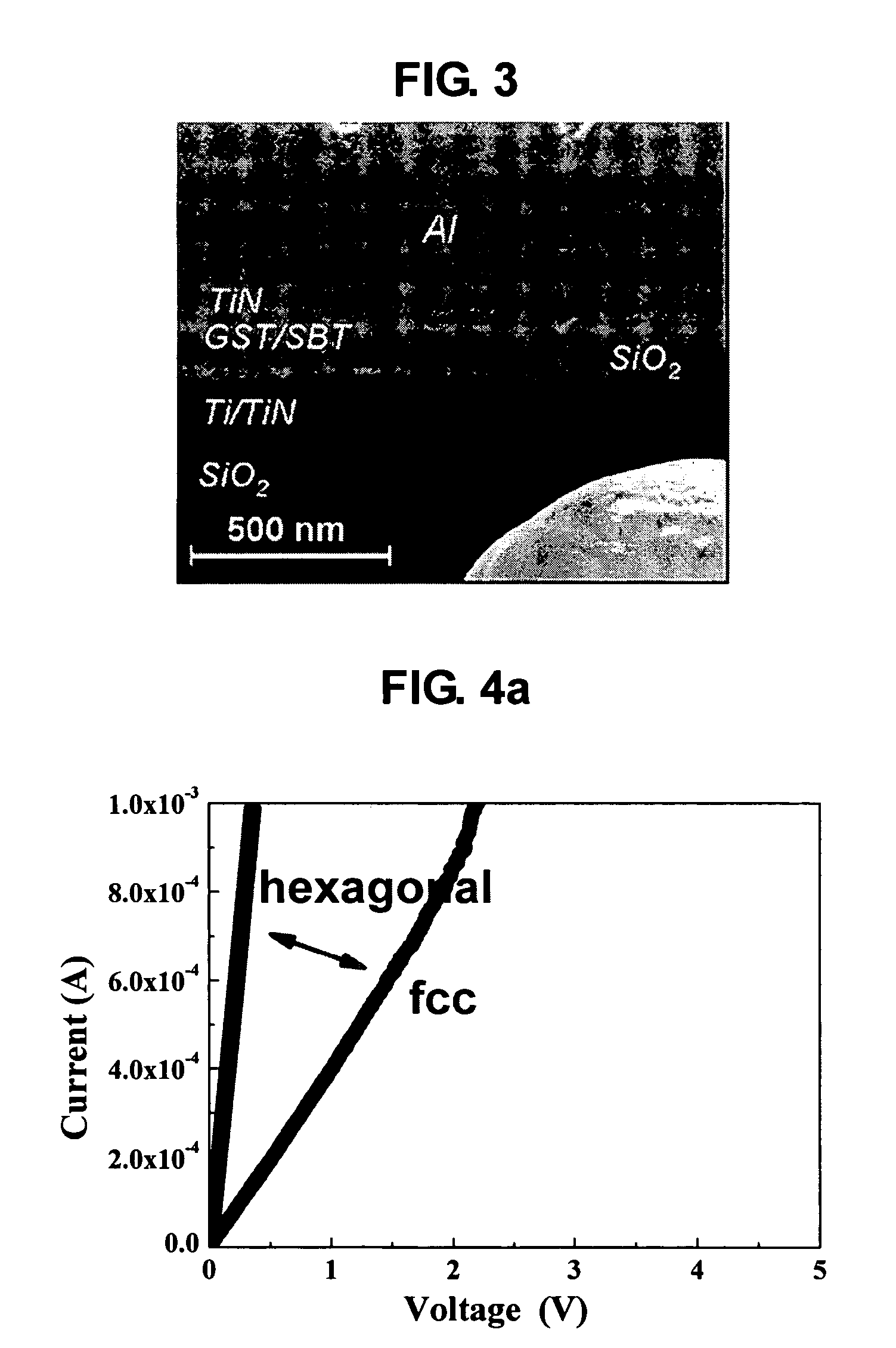
[0040]FIG. 3 illustrates sectional SEM picture of a phase change...

example 2

[0041] Procedures in Example 1 were repeated except that a solid solution of (Ge1Sb2Te4)0.9(Sn1Bi2Te4)0.1 was used instead of (Ge1Sb2Te4)0.8(Sn1Bi2Te4)0.2.


PUM

PropertyMeasurementUnit
thicknessaaaaaaaaaa
resistancesaaaaaaaaaa

Abstract

The present invention provides a phase change memory cell comprising (GeASbBTeC)1−x(RaSbTeC)x solid solution, the solid solution being formed from a Ge—Sb—Te based alloy and a ternary metal alloy R—S—Te sharing same crystal structure as the Ge—Sb—Te based alloy. A nonvolatile phase change memory cell in accordance with the present invention provides many advantages such as high speed, high data retention, and multi-bit operation.

Description

FIELD OF THE INVENTION [0001] The present invention relates to a non-volatile memory device using a phase change material. BACKGROUND OF THE INVENTION [0002] In recent years, there has been a renewal of interest in phase change random access memory (PCRAM) as a promising candidate for next generation nonvolatile memory device because of many advantages such as non-volatility, fast operation property, process simplicity and possibility of multi-bit operation. [0003] Traditionally, PCRAM employs a chalcogenide-based phase change material such as a stoichiometric Ge—Sb—Te alloy like Ge2Sb2Te5. A Ge—Sb—Te based alloy is capable of storing information in a binary form by electrically switching between the amorphous and crystalline states in a reversible manner. [0004] Despite its merits as nonvolatile phase change memory material, however, a Ge—Sb—Te based alloy is disadvantageous as it tends to yield slow writing speed. For instance, it takes about 100 ns for the completion of the phase...

Claims


Application Information

Patent Timeline
Patent Type & Authority Applications(United States)
IPC IPC(8): H01L29/02
CPCH01L45/06H01L45/1233H01L45/126H01L45/144H10N70/8413H10N70/231H10N70/8828H10N70/826
Inventor AHN, DONG HOLEE, TAE-YONKIM, KI BUMCHEONG, BYUNG-KIKANG, DAE-HWANJEONG, JEUNG-HYUNKIM, IN HOLEE, TAEK SUNGKIM, WON MOK
Owner SK HYNIX INC
Why Eureka
Try Eureka