

Electrochemical cell structure and method of fabrication
- Summary
- Abstract
- Description
- Claims
- Application Information
AI Technical Summary
Benefits of technology
Problems solved by technology
Method used
Image

Examples
Embodiment Construction
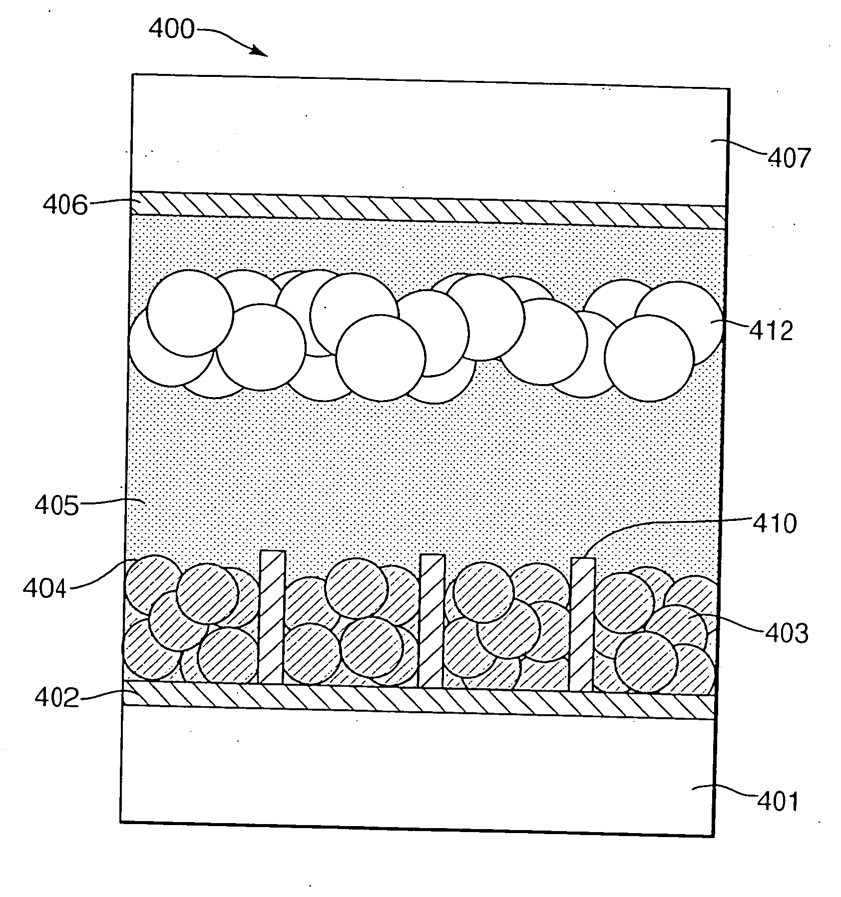
[0054] The present invention relates to an electrochemical cell such as a Dye Sensitised Solar Cell (DSSC) or an electrochromic display (ECD). One electrochemical cell 400 of the present invention comprises, with reference to FIG. 4, a first transparent insulating substrate layer 401; a first transparent conductive oxide (TCO) electrode layer 402; a metal oxide layer 403; a sensitiser (dye) / electrochromic material layer 404; an electrolyte layer 405; a second TCO electrode layer 406; and a second transparent insulating substrate layer 407.
[0055] The first and second transparent insulating substrate layers 401, 407 are preferably glass or plastic. The metal oxide layer 403 is preferably titanium dioxide (TiO2) and is a semiconductor.
[0056] The metal oxide layer 403 should preferably be a material which promotes intimate adhesion of the sensitiser (dye) / electrochromic material layer 404 on its surface. Additionally, the particles of the metal oxide layer 403 must be reasonably light...
PUM
 Abstract
Description
Claims
Application Information