Semiconductor components having through wire interconnects (TWI)

a technology of semiconductor components and wire interconnects, which is applied in the direction of semiconductor devices, semiconductor/solid-state device details, electrical apparatus, etc., can solve the problems of reducing the number of transistors, the inability of semiconductor components to be stacked, and the limitations of conventional interconnects, so as to reduce capacitance and noise

Active Publication Date: 2007-06-07
MICRON TECH INC
View PDF47 Cites 123 Cited by
  • Summary
  • Abstract
  • Description
  • Claims
  • Application Information

AI Technical Summary

Benefits of technology

[0009] Another stacked semiconductor component includes a plurality of stacked semiconductor substrates having bonded through wire interconnects on adjacent substrates. A wire bonded semiconductor component includes a package substrate, and a semiconductor substrate having a through wire interconnect wire bonded to the package substrate. A flip chip semiconductor component includes a package substrate, and a semiconductor substrate having a through wire interconnect flip chip bonded to the package substrate. A face to face stacked semiconductor component includes two components in a face to face configuration with terminal contacts on opposing sides. A back to back stacked semiconductor component includes two components in a back to back configuration with terminal contacts on opposing sides. With any stacked semiconductor component, at least some of the through wire interconnects can include electrically isolated substrate contacts, configured to reduce capacitance and noise on signals transmitted through the stacked semiconductor component.

Problems solved by technology

In general, conventional interconnects have limitations on conductivity, capacitance, density and manufacture.
Conventional interconnects also have limitations on their ability to form stacked semiconductor components.
Other limitations of the related art will become apparent to those of skill in the art upon a reading of the specification and a study of the drawings.

Method used


Image

  • Semiconductor components having through wire interconnects (TWI)
  • Semiconductor components having through wire interconnects (TWI)
  • Semiconductor components having through wire interconnects (TWI)

Examples


Embodiment Construction

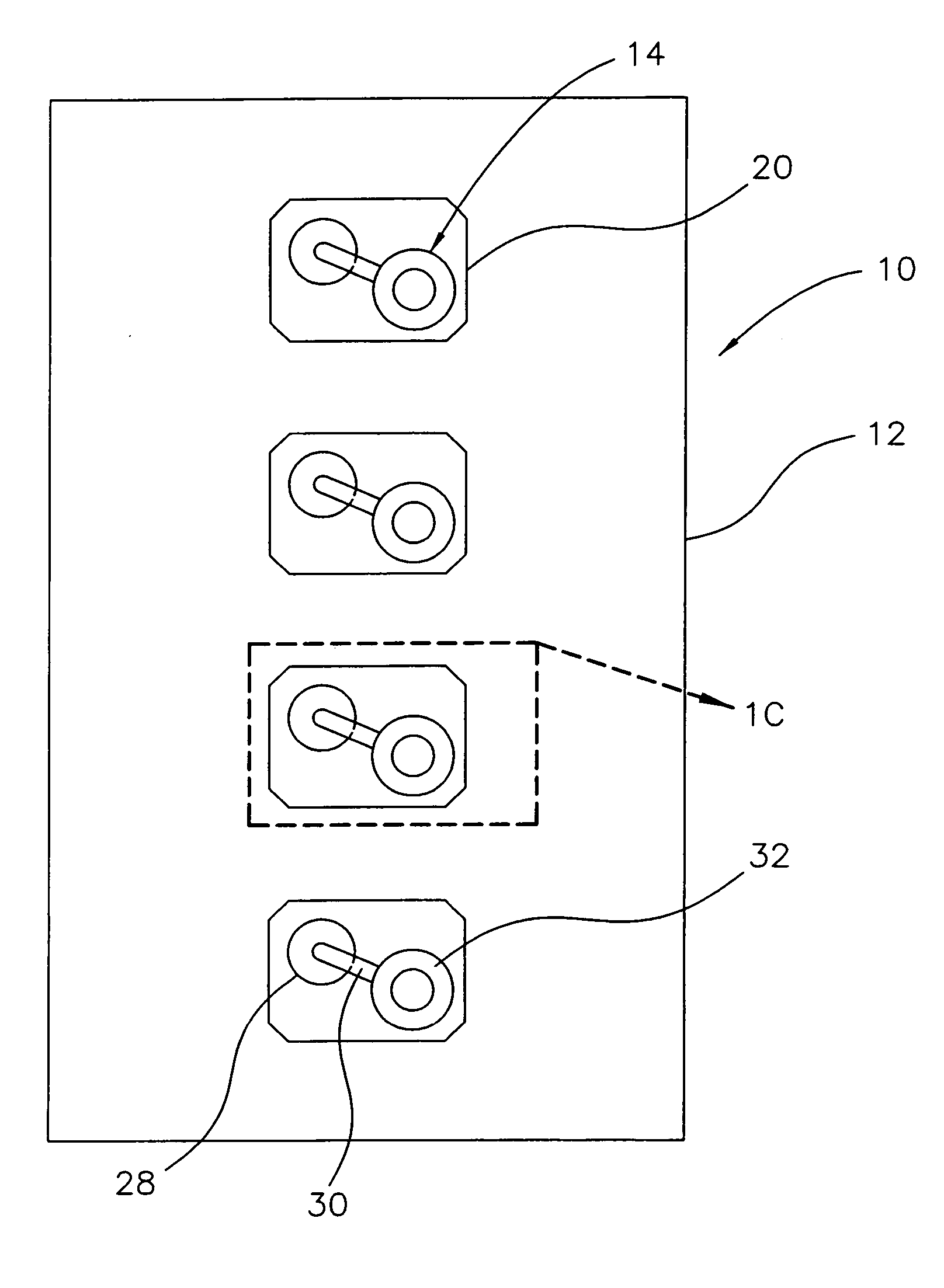
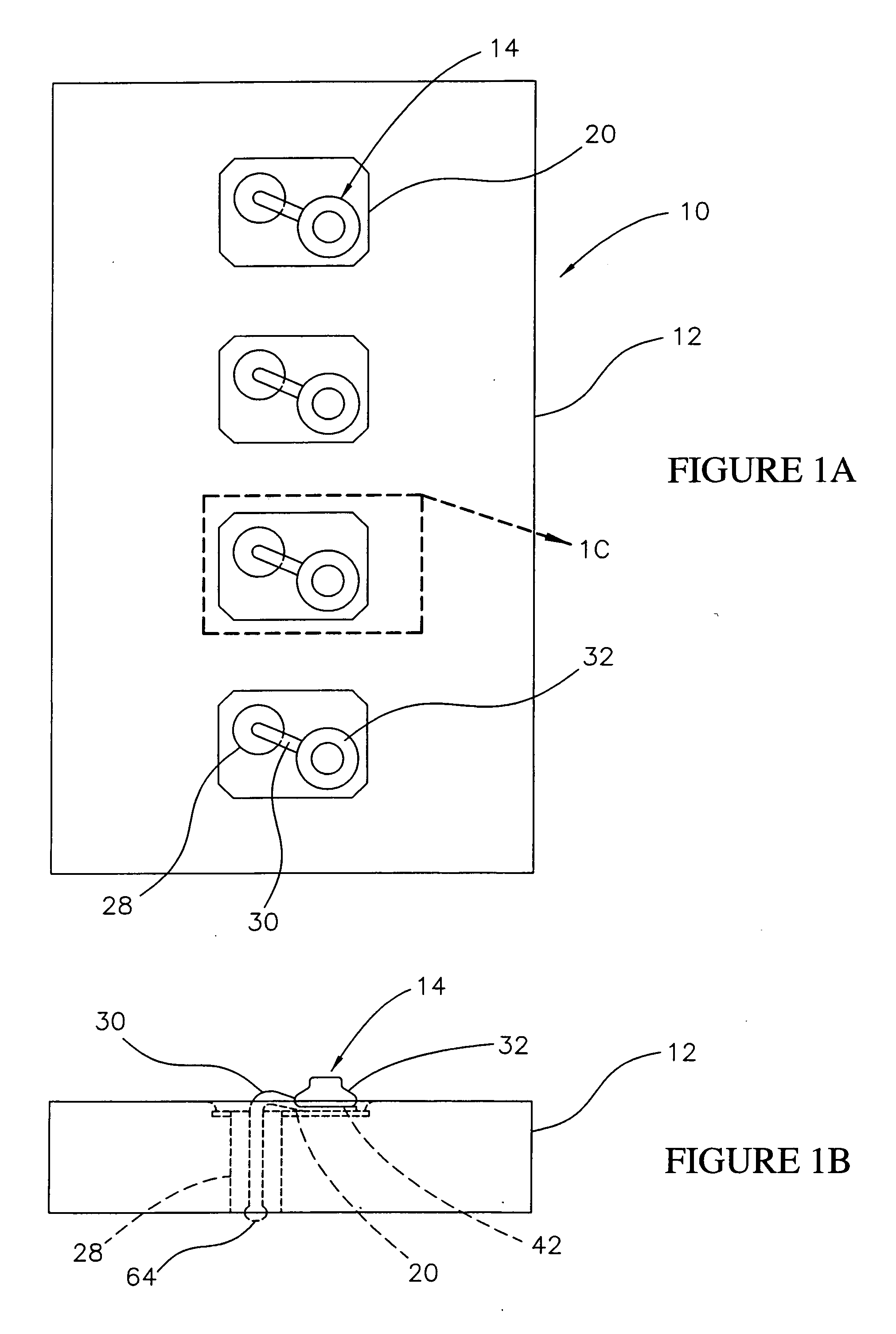
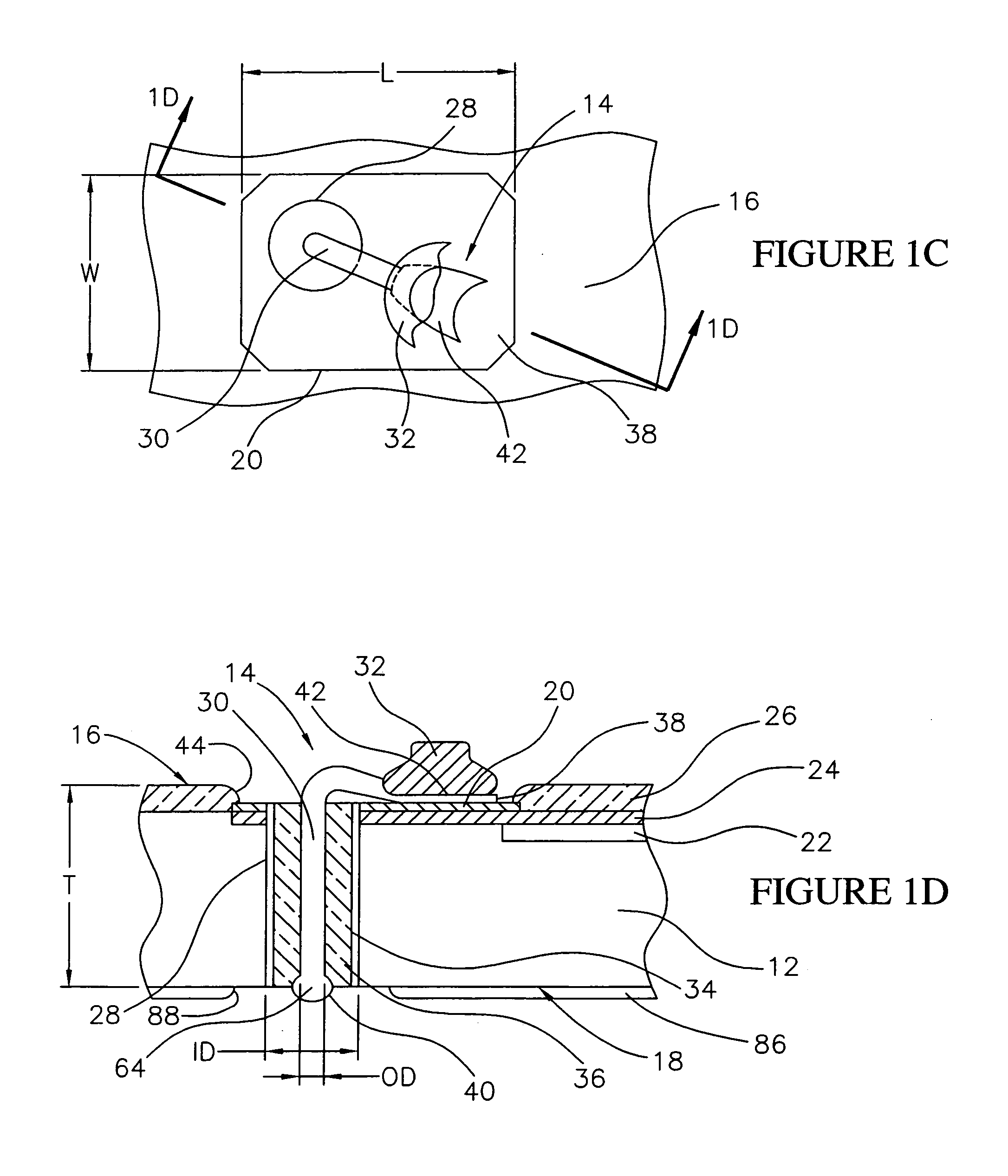
[0047] As used herein, “semiconductor component” means an electronic element that includes a semiconductor substrate. “Semiconductor substrate” means an electronic element, such as a semiconductor die, or a semiconductor package that includes integrated circuits and semiconductor devices. “Interconnect” means an electrical element which electrically connects different electrical elements and transmits signals between these elements. “Wafer-level” means a process conducted on an element, such as a semiconductor wafer, containing multiple semiconductor substrates. “Die level” means a process conducted on a singulated element, such as a singulated semiconductor die or package. “Chip scale” means having an outline about the same as that of a semiconductor die. “Wafer size” means having an outline about the same as that of a semiconductor wafer.

[0048] Referring to FIGS. 1A-1D, a semiconductor component 10 (FIG. 1A) is illustrated. The semiconductor component 10 (FIG. 1A) includes a semi...


PUM


Abstract

A semiconductor component includes a semiconductor substrate having a substrate contact, and a through wire interconnect (TWI) bonded to the substrate contact. The through wire interconnect (TWI) includes a via through the substrate contact and the substrate, a wire in the via bonded to the substrate contact, and a contact on the wire. A stacked semiconductor component includes the semiconductor substrate, and a second semiconductor substrate stacked on the substrate and bonded to a through wire interconnect on the substrate. A method for fabricating a semiconductor component with a through wire interconnect includes the steps of providing a semiconductor substrate with a substrate contact, forming a via through the substrate contact and part way through the substrate, placing the wire in the via, bonding the wire to the substrate contact, and then thinning the substrate from a second side to expose a contact on the wire. A system for fabricating the semiconductor component includes a bonding capillary configured to place the wire in the via, and to form a bonded connection between the wire and the substrate contact.

Description

BACKGROUND OF THE INVENTION [0001] As semiconductor components become smaller and have more complicated input / output configurations, different types of interconnects have been developed for implementing different signal transmission systems to and from the integrated circuits contained on the components. For example, surface interconnects, such as redistribution conductors can be formed on a particular surface, such as on a face or a back side of a semiconductor component. Via interconnects, such as metal filled vias, can be used to electrically connect electrical elements, such as terminal contacts or bond pads, on opposing surfaces of a semiconductor component. Wire interconnects, such as wires bonded to bond pads, can be used to electrically connect a semiconductor component to mating contacts on a supporting substrate, such as a package substrate, a module substrate, or a PCB. Bump interconnects, such as solder balls or bumps, can be used to mount a semiconductor component in a ...

Claims


Application Information

Patent Timeline
Patent Type & Authority Applications(United States)
IPC IPC(8): H01L23/495
CPCH01L21/6835H01L23/3114H01L23/481H01L23/49827H01L24/45H01L24/48H01L24/78H01L24/85H01L25/0657H01L2221/6834H01L2224/1134H01L2224/45014H01L2224/45015H01L2224/45139H01L2224/4554H01L2224/45565H01L2224/48091H01L2224/4813H01L2224/48145H01L2224/4824H01L2224/48471H01L2224/48475H01L2224/48599H01L2224/48699H01L2224/49429H01L2224/78301H01L2224/85001H01L2224/85045H01L2224/85051H01L2224/85121H01L2224/85205H01L2224/85951H01L2225/06506H01L2225/06513H01L2225/06524H01L2225/06541H01L2225/06596H01L2924/01012H01L2924/01013H01L2924/01014H01L2924/01027H01L2924/01028H01L2924/01029H01L2924/01031H01L2924/01046H01L2924/01047H01L2924/0105H01L2924/01074H01L2924/01078H01L2924/01079H01L2924/01082H01L2924/014H01L2924/14H01L2924/1433H01L2924/15311H01L2924/19042H01L2924/20751H01L2924/20752H01L2924/20753H01L2924/20754H01L2924/20755H01L2924/20756H01L2924/20757H01L2924/20758H01L2924/20759H01L2924/2076H01L2924/30105H01L2924/30107H01L2924/3011H01L2924/3025H01L24/49H01L2924/0102H01L2924/01033H01L2924/01043H01L2924/00015H01L2224/45124H01L24/10H01L2224/48992H01L2224/02372H01L2224/13024H01L2224/02335H01L2224/02333H01L24/11H01L24/13H01L2224/0401H01L2924/00014H01L2224/45144H01L2224/45147H01L2224/45644H01L2924/00H01L2924/12042H01L2224/11H01L2224/13H01L2224/85444H01L2224/85207H01L2924/2075H01L2924/013H01L2924/00013H01L2924/00012H01L2924/206H01L23/48H01L23/02
Inventor WOOD, ALAN G.HEMBREE, DAVID R.
Owner MICRON TECH INC
Why Eureka
Try Eureka