Current limited bilateral MOSFET switch with reduced switch resistance and lower manufacturing cost

a technology of mosfet switch and switch resistance, which is applied in the direction of electronic switching, emergency protective arrangements for limiting excess voltage/current, pulse technique, etc., can solve the problems of increasing the switching resistance, high resistance, and inconvenient implementation in devices where higher power efficiency is required

Active Publication Date: 2007-06-07
ALPHA & OMEGA SEMICON LTD
View PDF5 Cites 32 Cited by
  • Summary
  • Abstract
  • Description
  • Claims
  • Application Information

AI Technical Summary

Benefits of technology

[0015] Briefly in a preferred embodiment this invention discloses a current limited bilateral switch that includes two back-to-back field effect transistors (FETs) for switching off a current flow in an OFF state irrespective of a voltage polarity applied to the bilateral switch wherein one of the two back-to-back FET transistor further functioning as a sensed linear resistor. The bilateral switch further includes a current limit circuit for sensing and limiting a voltage across the one of the back-to-back FET transistors functioning as the sensed linear resistor. In a preferred embodiment, the two back-to-back FETs further having a drain-to-source resistance of Rdson and the current limited bilateral switch having a total resistance substantially equal to two times the resistance Rdson. In another preferred embodiment, the two back-to-back FETs further include two back-to-back common source P-FET transistors. In another preferred embodiment, the two back-to-back FETs further include two back-to-back common drain P-FET transistors. In another preferred embodiment, the two back-to-back FETs further include two back-to-back common source N-FET transistors. In another preferred embodiment, the two back-to-back FETs further include two back-to-back common drain N-FET transistors. In another preferred embodiment, the current limiting circuit further includes a current-limiting voltage generator having a limiting voltage Vlim for comparing with and limiting the voltage across the one of two back-to-back transistors functioning as the sensed linear resistor. In another preferred embodiment, the current-limiting voltage generator further includes a band-gap reference generator for providing the limiting voltage Vlim for comparing with and limiting the voltage across the one of two back-to-back transistors functioning as the sensed linear resistor. In another preferred embodiment, the current limiting circuit further includes a comparator for comparing the current-limiting voltage Vlim with the voltage across the one of two back-to-back transistors functioning as the sensed linear resistor.

Problems solved by technology

Conventional technologies and circuit designs for current limited bilateral switch implemented with FET based transistors are still limited by a technical difficulty that the switching resistance is high and cannot be conveniently implemented in device where higher power efficiency is required.
As will be further discussed below specifically, combinations of circuits employed to enable bilateral switch and also limiting the current often inadvertently increase the switching resistance.
The increase in switch resistance inevitably leads to the undesirable effects of power wastes, loss of efficiency and heat generations.
The technical difficulty thus limits the application of the FET-based bilateral switches to many applications while there are increasing demands to provide effective and conveniently integration FET based power devices and power switches.
Since the required charge pump for the NMOS gate drive often has high output impedance, when integrated into an IC, it is usually not possible to power the amplifier A1 directly from the charge pump.
However, such switches present a severe technical difficulty due to a high switch resistance when a switch is configured with such combination of circuits.
For high power applications, such bilateral switches often present high power consumption and low operational efficiency and would not be acceptable.

Method used


Image

  • Current limited bilateral MOSFET switch with reduced switch resistance and lower manufacturing cost
  • Current limited bilateral MOSFET switch with reduced switch resistance and lower manufacturing cost
  • Current limited bilateral MOSFET switch with reduced switch resistance and lower manufacturing cost

Examples


Embodiment Construction

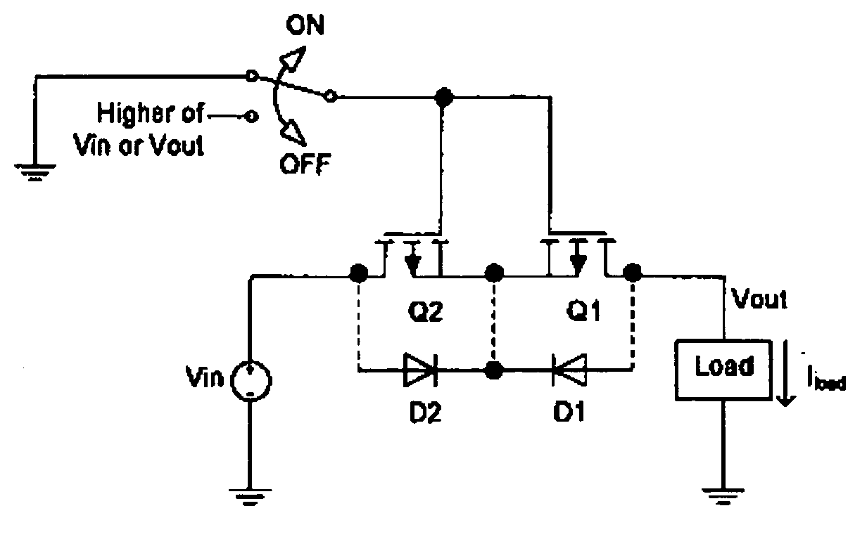
[0023] Referring to FIG. 5A for a circuit diagram for a new and improved current limited bilateral switch implemented with two common-source P-FET transistors to overcome the above-discussed technical difficulties. The current limited bilateral power switch 100 includes two common-source P-FET transistors 110 and 120 shown as Q1 and Q2 respectively with a common source node 125. The second P-FET bilaterally functional transistor 120 serves the functions of a sense resistor, e.g., Rs shown in FIGS. 4A. The voltage drop across the P-FET transistor 120 is sensed by an amplifier 130 shown as A1. The voltage drop across the P-FET transistor 120 is represented by a value of Iload×Rdson2 where Iload is the current passes through the load 140 and the Rdson2 is the resistance between the source and drain of the second P-FET transistor 120. The voltage drop across the P-FET transistor 120 is compared against a current-limiting voltage Vlim 150 that is implemented to prevent the current to exc...


PUM


Abstract

A circuit and method for controlling a MOSFET based switch that includes two back-to-back FET to block current flow in the OFF state irrespective of the polarity of the voltage differential across the switch. The MOSFET based switch further has a built-in current limit function by sensing the current flow through one of the two MOSFET switches. Furthermore, the bilateral current-limited switch further includes circuitry required for controlling both P type and N type FET in either common drain or common source configuration.

Description

BACKGROUND OF THE INVENTION [0001] 1. Field of the Invention [0002] The invention disclosed herein relates generally to the circuit design and configuration of power MOSFET based devices. More particularly, this invention relates to a novel and improved circuit configuration designs and manufacturing methods for providing current limited bi-lateral MOSFET switches. [0003] 2. Description of the Prior Art [0004] Conventional technologies and circuit designs for current limited bilateral switch implemented with FET based transistors are still limited by a technical difficulty that the switching resistance is high and cannot be conveniently implemented in device where higher power efficiency is required. As will be further discussed below specifically, combinations of circuits employed to enable bilateral switch and also limiting the current often inadvertently increase the switching resistance. The increase in switch resistance inevitably leads to the undesirable effects of power waste...

Claims


Application Information

Patent Timeline
Patent Type & Authority Applications(United States)
IPC IPC(8): H02H3/00
CPCH02H9/025H03K17/0822H03K17/6874H03K2217/0036
Inventor CHANG, ALLENWEI, ZHINAN
Owner ALPHA & OMEGA SEMICON LTD
Why Eureka
Try Eureka