Nitride semiconductor light emitting device and method for fabricating the same

a light emitting device and semiconductor technology, applied in semiconductor/solid-state device manufacturing, semiconductor devices, electrical equipment, etc., can solve the problems of increased cost low heat release, high cost of sapphire, etc., to improve electrical and optical characteristics and reliability of light emitting devices.

Active Publication Date: 2007-06-14
SUZHOU LEKIN SEMICON CO LTD
View PDF7 Cites 27 Cited by
  • Summary
  • Abstract
  • Description
  • Claims
  • Application Information

AI Technical Summary

Benefits of technology

[0017] Accordingly, the invention is related to a nitride semiconductor light emitting device and a method for fabricating the same, in which a nitride semiconductor is stacked on a silicon substrate, thereby improving electrical and optical characteristics and reliability of the light emitting device.

Problems solved by technology

The production cost of this sapphire is high, and thus the cost of the light emitting device is increased.
Further, the related sapphire substrate has low electrical and thermal conductivities in itself, and thus results in low heat release.
Hence, the light emitting device has a short lifetime, and is difficult to secure its reliability.
For this reason, the related sapphire substrate is impossible to fabricate micro-electromechanical system (MEMS) devices and micro optoelectronic integrated circuit (OEIC) devices having the photoelectric characteristic and a combination of electrical and electronic characteristics.

Method used


Image

  • Nitride semiconductor light emitting device and method for fabricating the same
  • Nitride semiconductor light emitting device and method for fabricating the same
  • Nitride semiconductor light emitting device and method for fabricating the same

Examples


Embodiment Construction

[0027] Hereinafter, a nitride semiconductor light emitting device and a method for fabricating the same in accordance with an embodiment of the present invention will be described in detail with reference to the accompanying drawings.

[0028] In the following description of an embodiment of the present invention, when a layer is formed “on” another layer, it may be formed directly on the other layer, or one or more intervening layer may be present.

[0029] Further, the light emitting device will be described as employing gallium nitride (GaN), but it is not limited to this. Therefore, the present invention can be applied to the nitride semiconductor light emitting device using groups 3 and 5 compounds such as gallium nitride (GaN), aluminum nitride (AlN), indium nitride (InN), and the like.

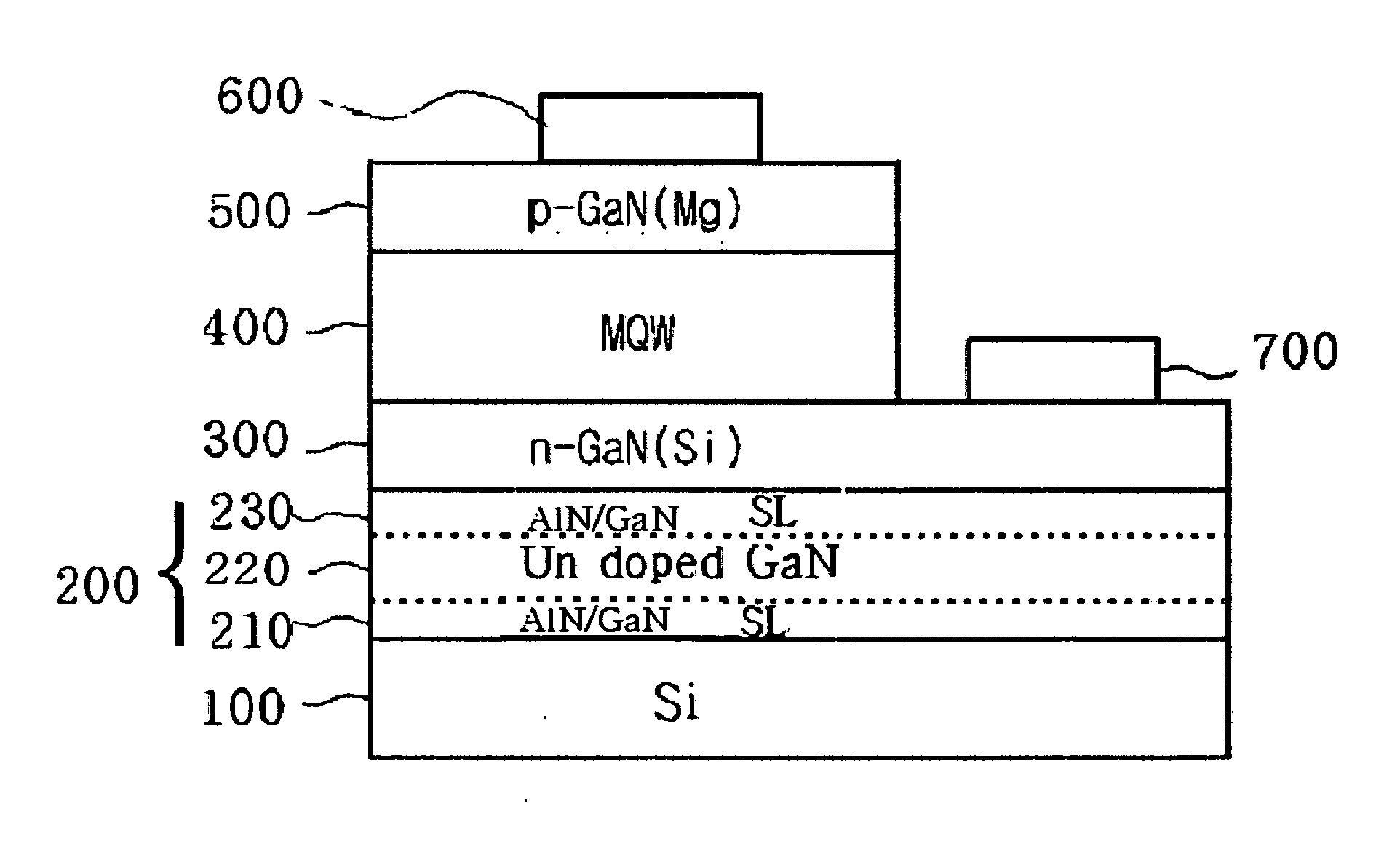
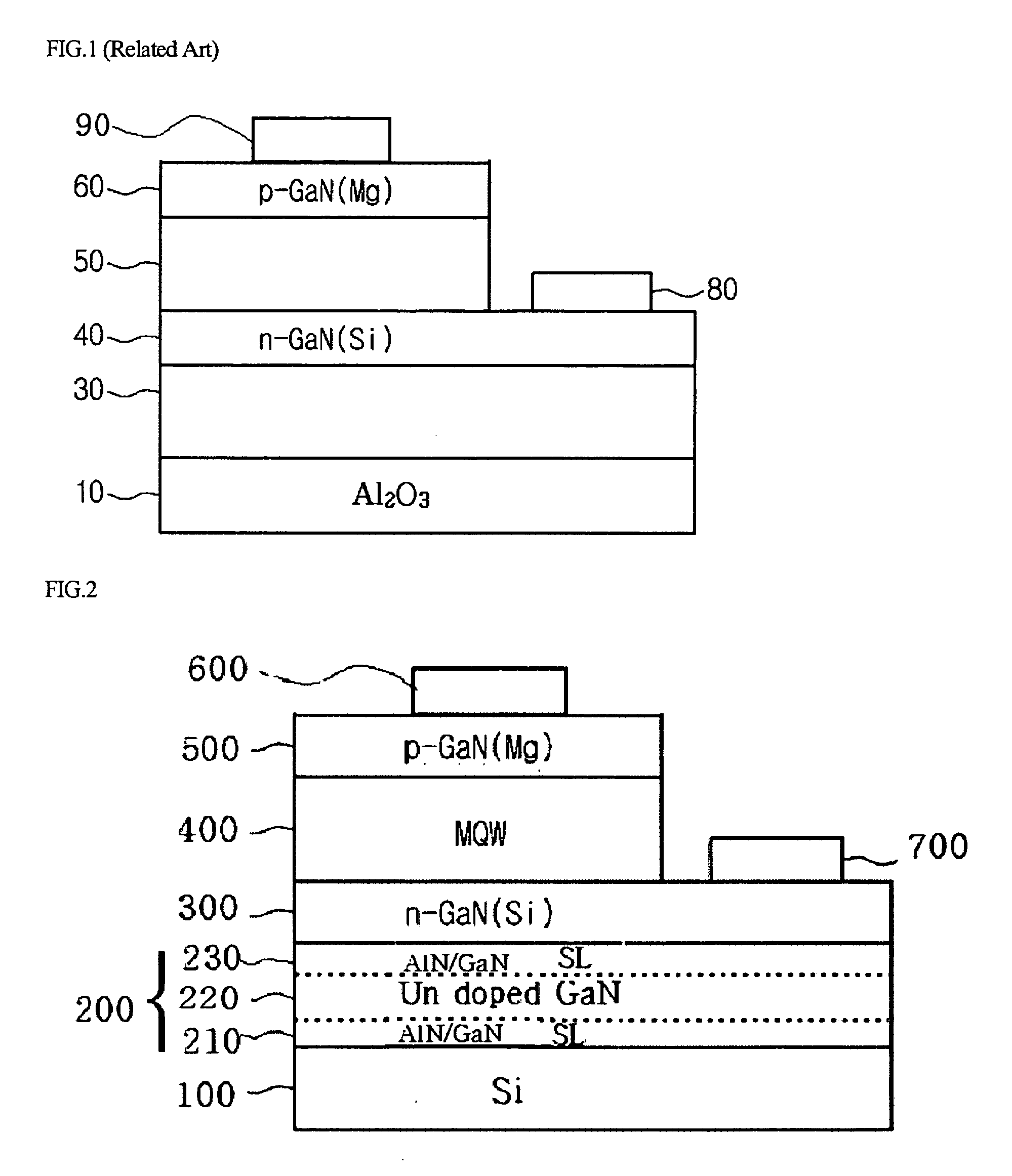
[0030]FIG. 2 is a sectional view illustrating a nitride semiconductor light emitting device according to an embodiment of the present invention.

[0031] As illustrated in FIG. 2, the nitride semicon...


PUM


Abstract

Disclosed is a nitride semiconductor light emitting device. The nitride semiconductor light emitting device comprises a buffer layer having a super-lattice layer on a silicon substrate, a first conductive clad layer on the buffer layer, an active layer on the first conductive clad layer, and a second conductive clad layer on the active layer.

Description

BACKGROUND OF THE INVENTION [0001] 1. Field of the Invention [0002] The present invention relates to a nitride semiconductor light emitting device and a method for fabricating the same. [0003] 2. Description of the Related Art [0004] Generally, a light emitting diode (LED) is one of the well-known semiconductor light emitting devices. The LED is used to send and receive signal by converting the electric signal into infrared radiation, visible radiation, or light using the characteristic of a compound semiconductor. [0005] The LED is used in various fields such as home electronics, remote controllers, electronic display boards, indicators, automated machines, and so on, and is generally classified into an infrared emitting diode and a visible light emitting diode. [0006] Typically, the downsized LED is made in the type of a surface mount device in order to directly mount it on a printed circuit board. Thus, an LED lamp used as a display device is being developed in the surface mount ...

Claims


Application Information

Patent Timeline
Patent Type & Authority Applications(United States)
IPC IPC(8): H01L33/00H01L33/04H01L33/06H01L33/12
CPCH01L33/007H01L33/04H01L33/06H01L33/12
Inventor SHIM, SANG KYUN
Owner SUZHOU LEKIN SEMICON CO LTD
Why Eureka
Try Eureka