Vertical image sensor and method for manufacturing the same

a technology of vertical image sensor and manufacturing method, which is applied in the field of vertical color filter detector group, can solve the problems of reducing the efficiency of blue light color reproduction, reducing the entire pixel area of light detection, and complex process, so as to reduce the area of the unit pixel, simplify the active pixel sensor circuit, and increase the aperture ratio

Inactive Publication Date: 2007-06-14
DONGBU ELECTRONICS CO LTD
View PDF7 Cites 58 Cited by
  • Summary
  • Abstract
  • Description
  • Claims
  • Application Information

AI Technical Summary

Benefits of technology

[0015] It is another object of the present invention to provide a vertical image sensor and a method for manufacturing the same, capable of simplifying an active pixel sensor circuit that senses signal charges from RGB layers by reducing the number of the active pixel sensor circuits from three to one and increasing an aperture ratio (the efficiency of a detection area) by reducing an area of the unit pixel for the active pixel sensor circuit.
[0016] In addition, it is still another object of the present invention to provide a vertical image sensor and a method for manufacturing the same, capable of simplifying a manufacturing process by reducing the number of ion implantations and masks used to form a path for connecting a green sensitive layer and a red sensitive layer to an active pixel sensor circuit on a surface of a silicon substrate.

Problems solved by technology

However, blue light is absorbed at a depth of only about 0.3 μm (that is, 3000 Å) under the surface of silicon, thereby reducing an efficiency of the color reproduction of blue light.
However, these APS circuits cause the expansion of a transistor area in each pixel area, thereby reducing a light detection area (or a proportion thereof) in the entire pixel area.
However, this makes a manufacturing process complex, thereby increasing manufacturing costs.

Method used


Image

  • Vertical image sensor and method for manufacturing the same
  • Vertical image sensor and method for manufacturing the same
  • Vertical image sensor and method for manufacturing the same

Examples


Embodiment Construction

[0034] Hereinafter, a vertical image sensor and a method for manufacturing the same according to the present invention will be described with respect to accompanying drawings.

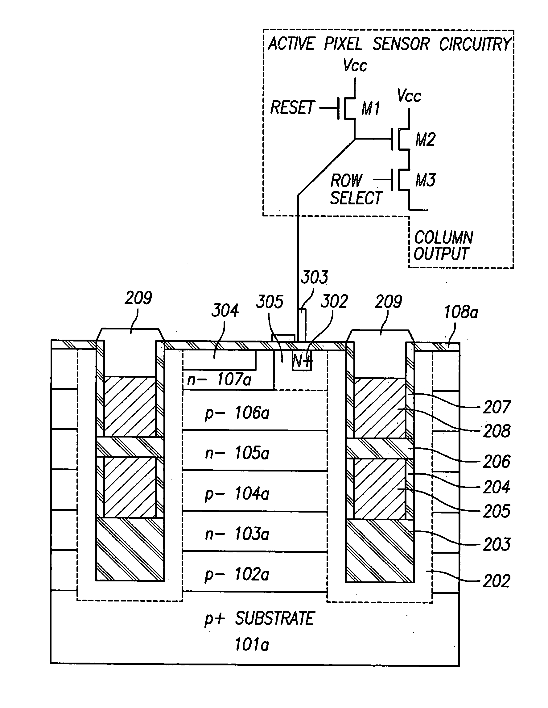
[0035]FIG. 5 is a sectional view showing the structure of a vertical color detector group (image sensor) having a trench-type charge transfer gate according to the present invention. As shown in FIG. 5, the vertical image sensor for detecting charges by a transistor having a trench-type gate includes a second conductive type blue-sensitive layer 107a which is formed on the upper surface of a first conductive type (P-type) semiconductor substrate 101 including a single crystal p+ substrate 101a, a second conductive green-sensitive layer 105a below the second conductive type blue-sensitive layer 107a, and a second conductive type red-sensitive layer 103a below the second conductive type green-sensitive layer 105a. In addition, the vertical image sensor includes a first silicon epitaxial layer 102a, a second sili...


PUM


Abstract

Disclosed are a vertical color filter detector group (image sensor) and a method for manufacturing the same, capable of simplifying a manufacturing process by reducing the number of ion implantations and masks for connecting a green sensitive layer and a red sensitive layer to a sensor on a surface of a silicon substrate. The image sensor includes a semiconductor substrate on which first and second conductive type silicon layers are stacked, and having at least two second conductive type regions at different depths from the semiconductor surface, a trench having a bottom lower than a first region farthest away from the semiconductor surface, to set a peripheral border area of a unit pixel, an insulating layer in the trench in contact with an interfacial surface between the semiconductor and the trench, a channel area in an active area between the first and second regions without contacting the interfacial surface between the semiconductor and the trench, and a transfer gate in the insulating layer.

Description

[0001] This application claims the benefit of Korean Application No. 10-2005-0120643, filed on Dec. 9, 2005, which is incorporated by reference herein in its entirety. BACKGROUND OF THE INVENTION [0002] 1. Field of the Invention [0003] The present invention relates to an image sensor. More specifically, the present invention relates to a vertical color filter detector group (image sensor) and a method for manufacturing the same, capable of simplifying a structure and a manufacturing process of the vertical image sensor. [0004] 2. Description of the Related Art [0005] Generally, a vertical image sensor includes six or more N-type layers and P-type layers formed on a semiconductor substrate. PN junctions formed by the N-type layers and the P-type layers (e.g., at an interface thereof) have various absorption rates for wavelengths of light, depending on the depth of the junctions. Accordingly, since the absorption rates for wavelengths of light vary according to the position of the PN ...

Claims


Application Information

Patent Timeline
Patent Type & Authority Applications(United States)
IPC IPC(8): H01L31/113H01L27/14H01L27/146H04N5/335H04N5/369H04N9/07
CPCH01L27/14603H01L27/14621H01L27/14647H01L27/14683H01L27/14689H01L27/146H01L27/15
Inventor KIM, JONG MIN
Owner DONGBU ELECTRONICS CO LTD
Why Eureka
Try Eureka