

Stacked semiconductor device
a semiconductor device and stacked technology, applied in semiconductor devices, semiconductor/solid-state device details, instruments, etc., can solve the problems and achieve the effect of reducing the yield of stacked semiconductor devices and high yield
- Summary
- Abstract
- Description
- Claims
- Application Information
AI Technical Summary
Benefits of technology
Problems solved by technology
Method used
Image

Examples
example 1
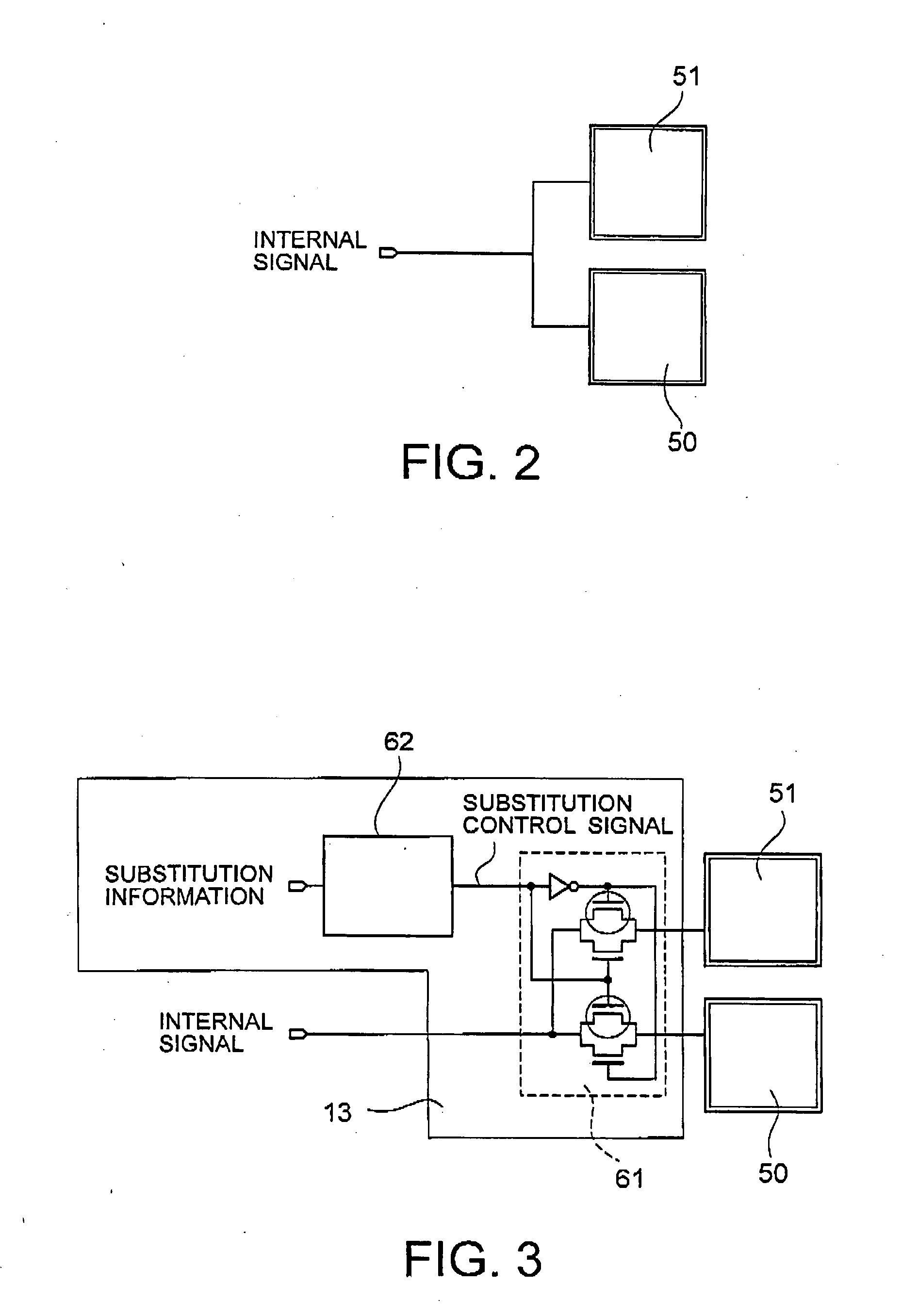
[0043] A basic configuration of a defective contact recovery means of through electrodes in Example 1 will be described with reference to FIGS. 2 to 4. FIG. 2 shows a recovery system in which one auxiliary through electrode 51 is provided as a defective contact recovery means for one signal line and arranged in parallel to a primary through electrode 50. FIG. 3 shows a recovery system in which one auxiliary through electrode 51 is provided for one signal line and a defective contact recovery circuit 13 is used to switch between a primary through electrode 50 and the auxiliary through electrode 51. FIG. 4 shows a recovery system in which one auxiliary through electrode 51 is provided for a plurality of signal lines and a defective contact recovery circuit 13 is used to switch between primary through electrodes 50 and the auxiliary through electrode 51.
[0044] The defective contact recovery means include a parallel arrangement recovery system using the same signal contact groups arran...
example 2
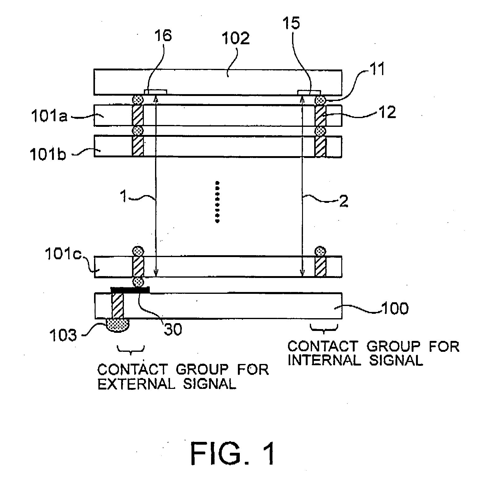
[0052] A stacked semiconductor device to which a defective contact recovery system is applied will be described as Example 2 with reference to FIGS. 5 to 8. FIG. 5 is a cross-sectional view showing a stacked semiconductor device in Example 2. FIG. 6 is an explanation diagram showing signal paths in the stacked semiconductor device shown in FIG. 5. FIG. 7 is a cross-sectional view showing locations of defective contacts in the stacked semiconductor device shown in FIG. 5. FIG. 8 is an explanation diagram showing signal paths in the stacked semiconductor device shown in FIG. 7.
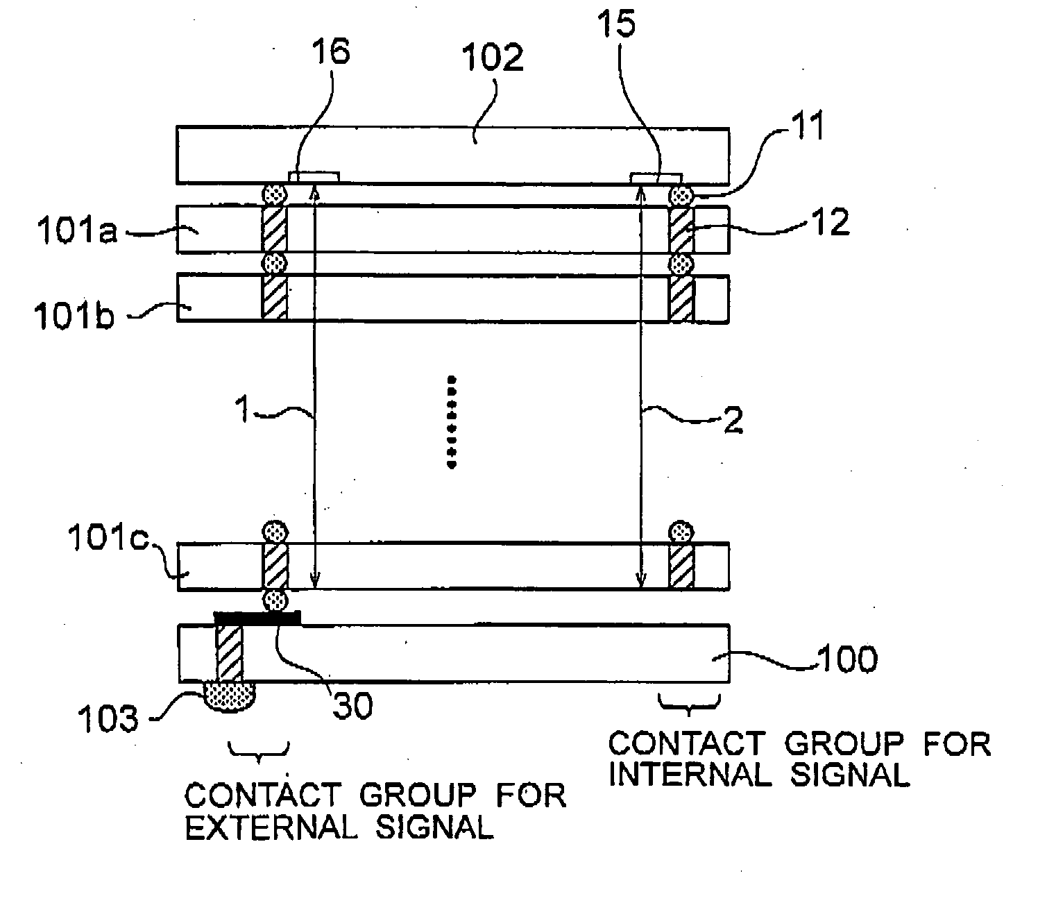
[0053] As shown in FIG. 5, the stacked semiconductor memory device comprises an interface chip 102, a plurality of core chips 101a to 101c, and an interposer 100. Each of the core chips 101a, 101b, and 101c has a large number of memory cells such as DRAMs, a circuit for storing data in the memory cells, and a control circuit for the memory cells and the aforementioned circuit. Specifically, each of the core chi...
example 3
[0068] A stacked semiconductor device to which the defective contact recovery means is applied will be described as Example 3 with reference to FIGS. 9 and 10. FIG. 9 is a cross-sectional view showing a stacked semiconductor device in Example 3. FIG. 10 is an explanation diagram showing signal paths in the stacked semiconductor device shown in FIG. 9.
[0069] As shown in FIG. 9, Example 3 differs from Example 1 in a stacked structure of an interface chip, core chips, and an interposer. In Example 3, an interposer 100 is stacked on an interface chip 102. Core chips 101a, 101b, and 101c are stacked on the interposer 100. The core chips 101a, 101b, and 101c are connected to each other by contact portions 11 between the chips and through electrodes 12. The connection produces signal paths 1 to 5 each formed by the contact portions 11 between the chips and the through electrodes 12. The signal paths 1 to 5 are used to transmit and receive signals between the core chips 101a to 101c and be...
PUM
 Abstract
Description
Claims
Application Information