Wafer dividing method

Inactive Publication Date: 2007-06-21
DISCO CORP
View PDF6 Cites 13 Cited by
  • Summary
  • Abstract
  • Description
  • Claims
  • Application Information

AI Technical Summary

Benefits of technology

[0016] In the wafer dividing method of the present invention, after the laminate formed at the streets of the wafer is divided along the streets by carrying out the laminate dividing step and the deteriorated layer is formed in the inside of the substrate along the streets by carrying out the deteriorated layer forming step, the wafer is divided along the streets by exerting external force to the wafer where

Problems solved by technology

Therefore, when devices formed on the wafer are small in size, the area ratio of the streets becomes large, thereby reducing productivity.
However, when a wafer having a low-dielectric constant insulating film (Low-k film) on the front surface or a wafer having a metal pattern composed of a metal f

Method used


Image

  • Wafer dividing method
  • Wafer dividing method
  • Wafer dividing method

Examples


first embodiment

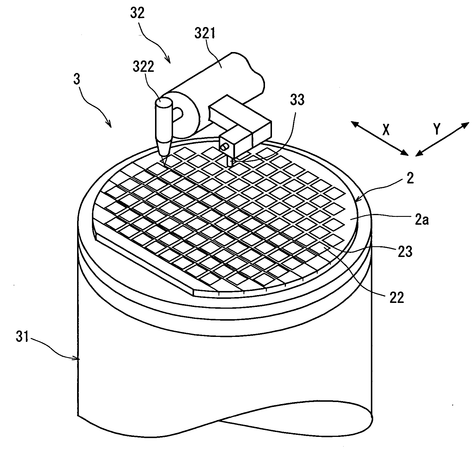
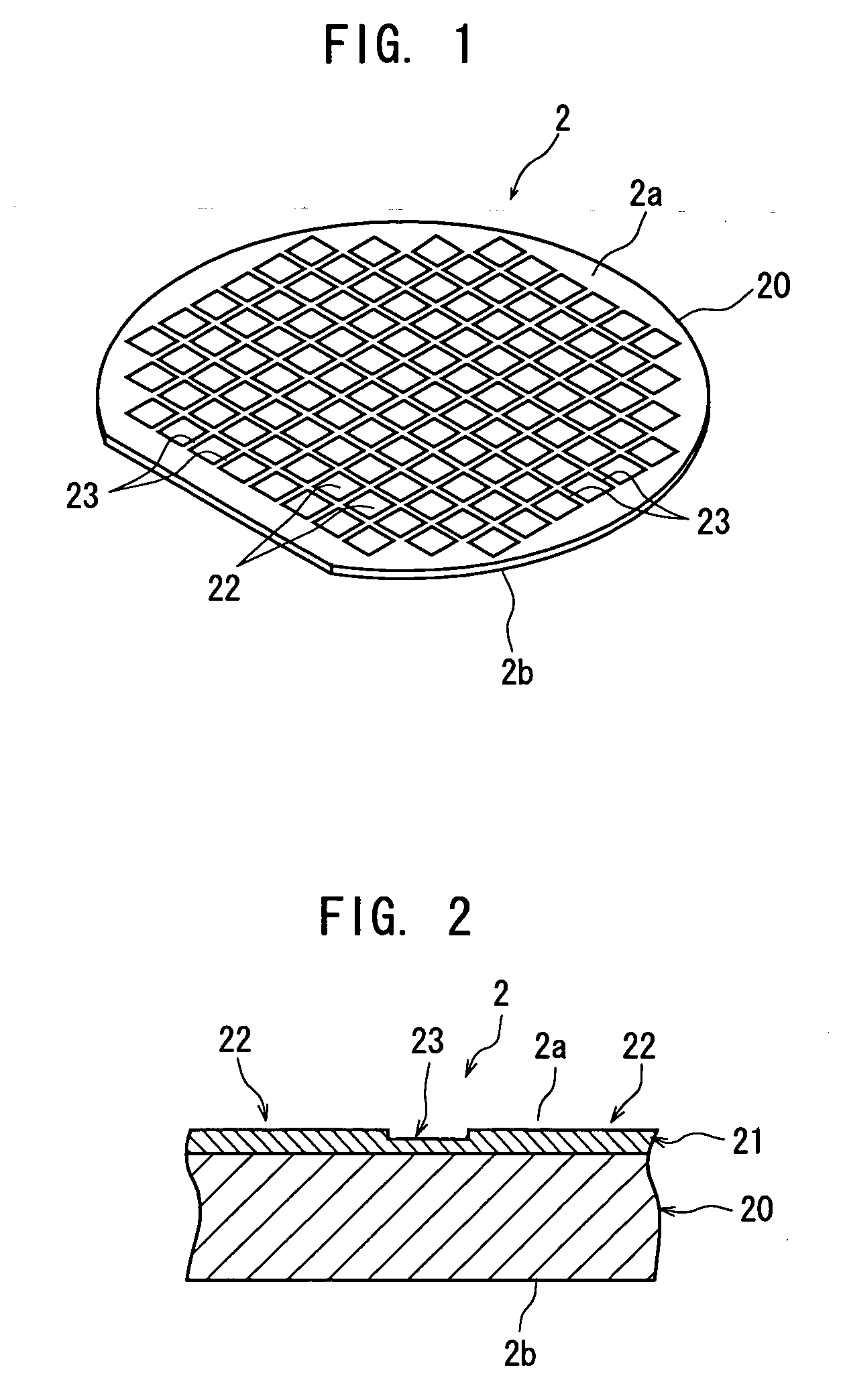
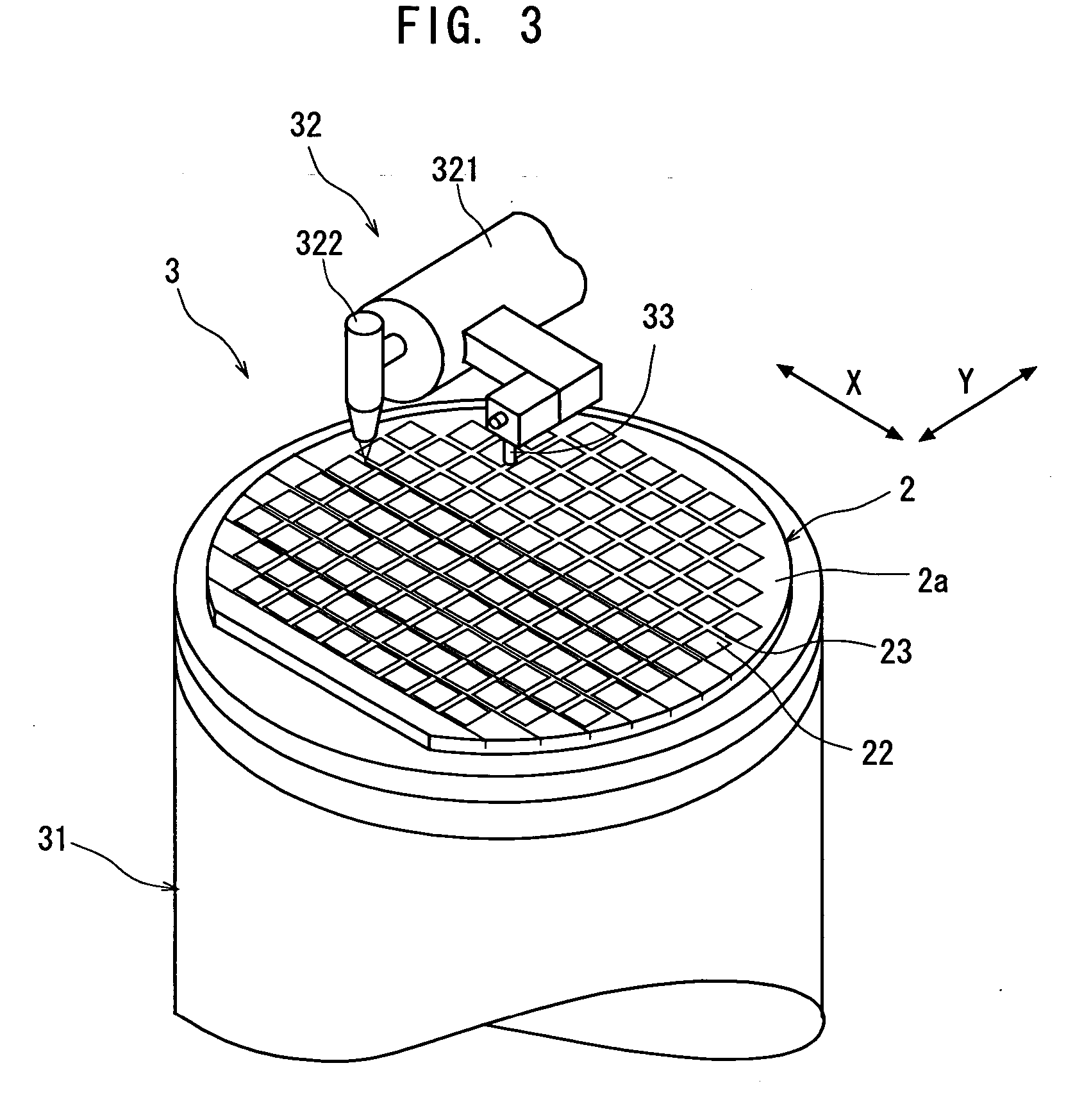
[0033] the method of dividing the above semiconductor wafer 2 along the streets 23 will be described with reference to FIG. 3 to FIG. 14.

[0034] In the first embodiment, the step of dividing the laminate 21 formed at the streets 23 of the semiconductor wafer 2 along the streets 23 is first carried out. This laminate dividing step is carried out by using a laser beam processing machine 3 shown in FIG. 3. The laser beam processing machine 3 shown in FIG. 3 comprises a chuck table 31 for holding a workpiece, a laser beam application means 32 for applying a laser beam to the workpiece held on the chuck table 31, and an image pick-up means 33 for picking up an image of the workpiece held on the chuck table 31. The chuck table 31 is designed to suction-hold the workpiece and to be moved in the processing-feed direction indicated by an arrow X and the indexing-feed direction indicated by an arrow Y in FIG. 3 by a moving mechanism that is not shown.

[0035] The above laser beam application me...

second embodiment

[0082] the method of dividing the above semiconductor wafer 2 along the streets 23 will be described hereinunder.

[0083] In the second embodiment, the step of forming a deteriorated layer in the inside of the semiconductor substrate 20 along the streets 23 by applying a laser beam having permeability for the semiconductor substrate 20 of the semiconductor wafer 2 from the rear surface 2b side of the semiconductor substrate 20 along the streets 23 is first carried out. This deteriorated layer forming step can be carried out in the same manner as the deteriorated layer forming step which is shown in FIGS. 9 to 11 by using a laser beam processing machine which is constituted substantially the same as the laser beam processing machine 3 shown in FIG. 3. At this point, the laser-processed groove 24 or the scribed groove 25 is not formed along the streets 23 in the semiconductor wafer 2.

[0084] After the above deteriorated forming step, next comes the step of putting the rear surface 2b si...


PUM

PropertyMeasurementUnit
Thicknessaaaaaaaaaa
Permeabilityaaaaaaaaaa

Abstract

A method of dividing a wafer having devices which are composed of a laminate formed on the front surface of a substrate, along a plurality of streets for sectioning the devices, comprising: a laminate dividing step for dividing the laminate formed at the streets of the wafer along the streets; a deteriorated layer forming step for forming a deteriorated layer in the inside of the substrate along the streets by applying a laser beam of a wavelength having permeability for the substrate of the wafer to the rear surface of the wafer along the streets; and a dividing step for dividing the wafer along the streets by exerting external force to the wafer where the deteriorated layers have been formed.

Description

FIELD OF THE INVENTION [0001] The present invention relates to a method of dividing a wafer having devices which are composed of a laminate formed on the front surface of a substrate, along a plurality of streets for sectioning the devices. DESCRIPTION OF THE PRIOR ART [0002] As is known to people of ordinary skill in the art, a semiconductor wafer having a plurality of semiconductor chips such as IC's or LSI's which are formed in a matrix on the front surface of a semiconductor substrate such as a silicon substrate and composed of a laminate consisting of an insulating film and a functional film is manufactured in the production process of a semiconductor device. The above semiconductor chips are sectioned by dividing lines called “streets” in this semiconductor wafer, and individual semiconductor chips are manufactured by dividing the semiconductor wafer along the streets. [0003] To improve the throughput of a semiconductor chip such as IC or LSI recently, a semiconductor wafer ha...

Claims


Application Information

Patent Timeline
IPC IPC(8): H01L21/00
CPCB23K26/0057B23K26/4075B28D5/0011H01L21/67092H01L21/78B23K26/40B23K26/53B23K2103/50
Inventor NAKAMURA, MASARU
Owner DISCO CORP
Why Eureka
Try Eureka