Low optical loss electrode structures for LEDs

a technology of low optical loss and electrode structure, applied in the direction of lasers, semiconductor lasers, solid-state devices, etc., can solve the problems of limiting the ability of contemporary leds to function in some applications, reducing the overall effectiveness and desirability of such contemporary leds, and reducing the brightness and/or efficiency of leds, so as to enhance the utility of leds. , the effect of increasing the brightness and/or efficiency

Active Publication Date: 2007-06-28
BRIDGELUX INC
View PDF13 Cites 112 Cited by
  • Summary
  • Abstract
  • Description
  • Claims
  • Application Information

AI Technical Summary

Benefits of technology

[0021] Thus, according to one or more embodiments of the present invention a brighter and/or more efficient LED can be provided. Increasing th...

Problems solved by technology

Although such contemporary LEDs have proven generally suitable for their intended purposes, they possess inherent deficiencies that detract from their overall effectiveness and desirability.
For example, the light output of such contemporary LEDs is not as great as is sometimes desired.
This limits the ability of contemporary LEDs to function in some applications, such as providing general illumination, e.g., ambient lighting.
Even high power contemporary LEDs do not provide sufficient illumination for such purposes.
At least a part of t...

Method used


Image

  • Low optical loss electrode structures for LEDs
  • Low optical loss electrode structures for LEDs
  • Low optical loss electrode structures for LEDs

Examples


Embodiment Construction

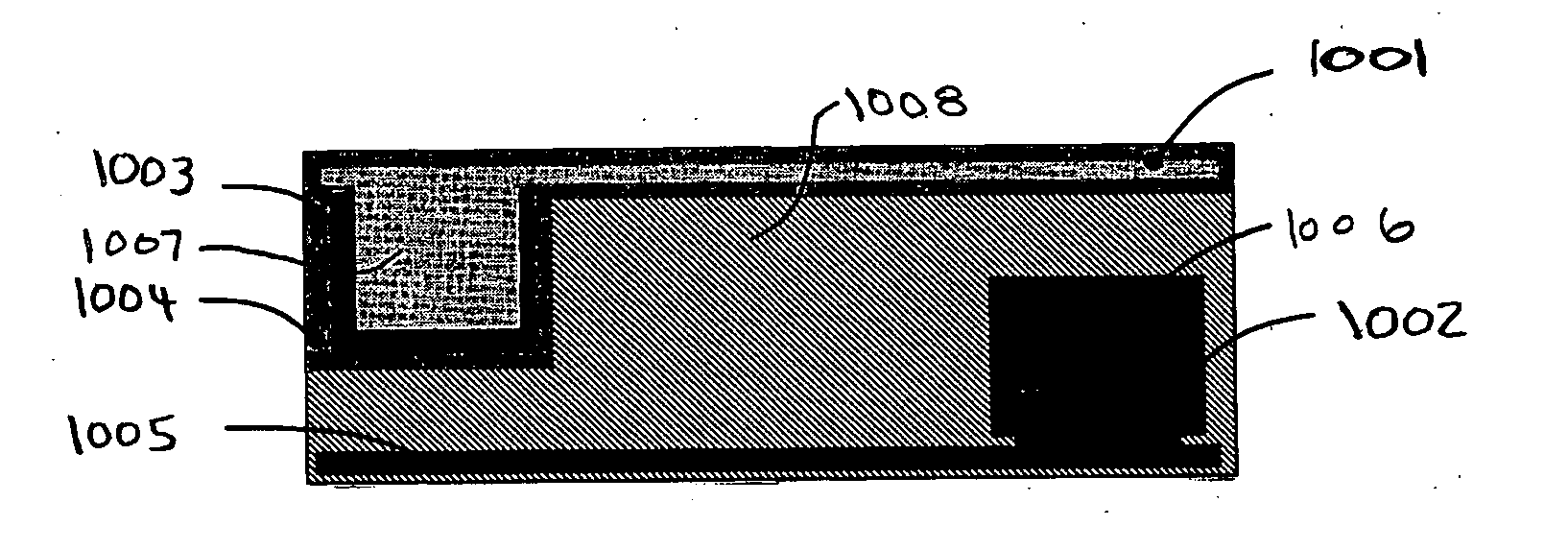
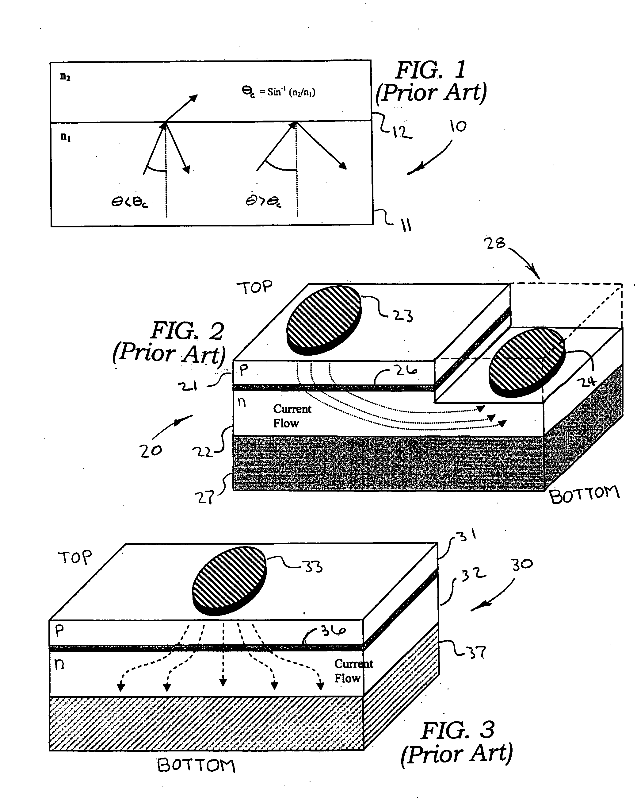
[0079] Light emitting devices (LEDs) emit light in response to excitation by an electrical current. One typical LED has a heterostructure grown on a substrate by metal-organic vapor phase epitaxy or a similar technique. An LED heterostructure includes n-type and p-type semiconductor layers that sandwich a light producing layer, i.e., an active region. Exemplary active areas may be quantum wells surrounded by barrier layers. Typically, electrical contacts are attached to the n-type and p-type semiconductor layers. When a forward bias is applied across the electrical contacts electrons and holes flow from n-type and p-type layers to produce light in the active region. Light is produced according to well known principles when these electrons and holes recombine with each other in the active region.

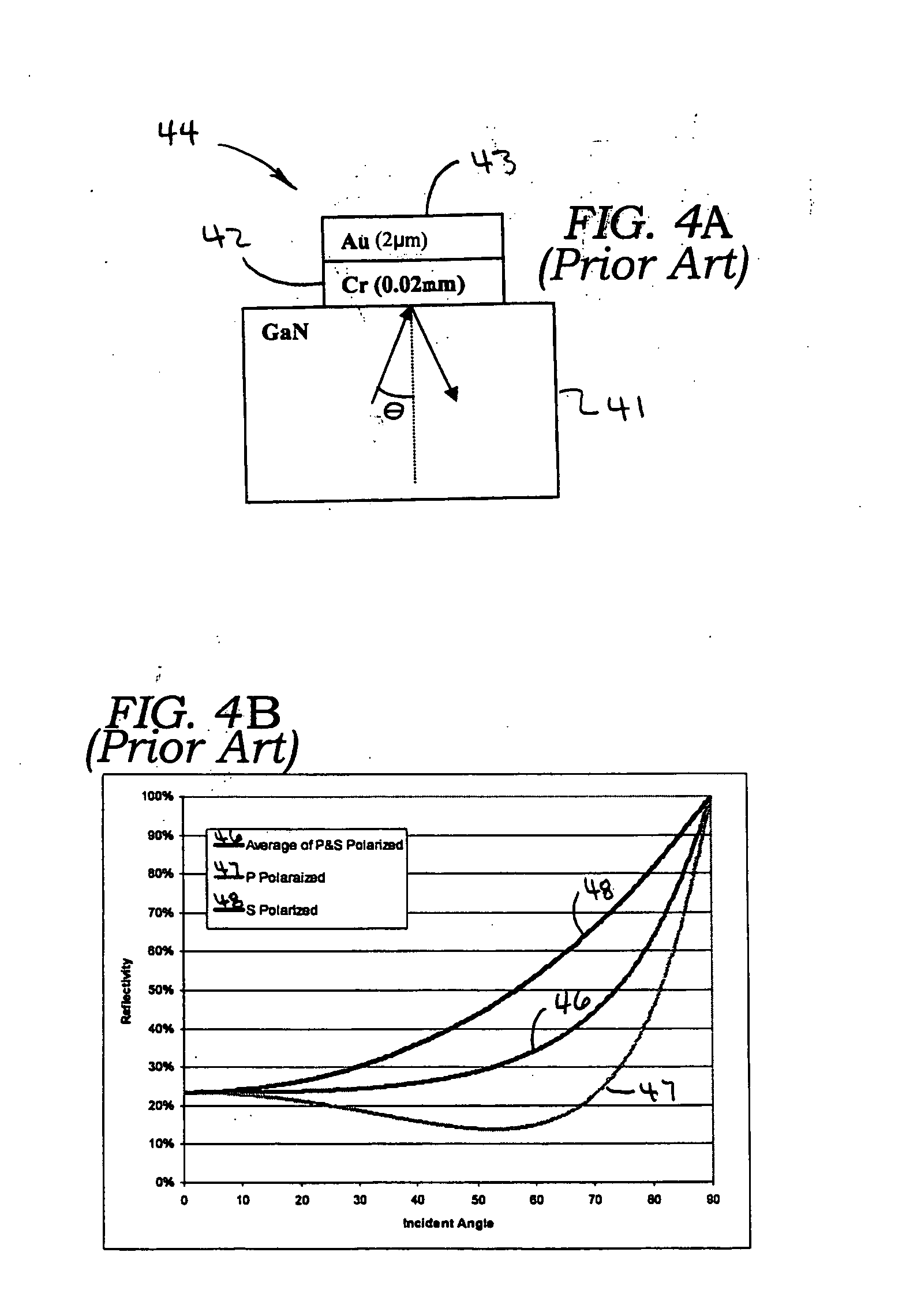
[0080] The efficiency with which a LED converts electricity to light is determined by the product of the internal quantum efficiency, the light-extraction efficiency, and losses due to elect...


PUM


Abstract

An electrode structure is disclosed for enhancing the brightness and/or efficiency of an LED. The electrode structure can have a metal electrode and an optically transmissive thick dielectric material formed intermediate the electrode and a light emitting semiconductor material. The electrode and the thick dielectric cooperate to reflect light from the semiconductor material back into the semiconductor so as to enhance the likelihood of the light ultimately being transmitted from the semiconductor material. Such LED can have enhanced utility and can be suitable for uses such as general illumination.

Description

TECHNICAL FIELD [0001] The present invention relates generally to light emitting diodes (LEDs). The present invention relates more particularly to electrode structures that mitigate optical losses and thus tend to enhance the brightness and / or the efficiency of LEDs. BACKGROUND [0002] Light emitting diodes (LEDs) for use as indicators are well known. LEDs have been used extensively for this purpose in consumer electronics. For example, red LEDs are commonly used to indicate that power has been applied to such devices as radios, televisions, video recorders (VCRs), and the like. [0003] Although such contemporary LEDs have proven generally suitable for their intended purposes, they possess inherent deficiencies that detract from their overall effectiveness and desirability. For example, the light output of such contemporary LEDs is not as great as is sometimes desired. This limits the ability of contemporary LEDs to function in some applications, such as providing general illumination...

Claims


Application Information

Patent Timeline
IPC IPC(8): H01L33/00H01L31/12H01L27/15H01L33/38H01L33/40H01L33/44H01L33/46
CPCH01L33/385H01L33/387H01L33/405H01L33/42H01L33/382H01L33/46H01L33/32H01L33/20H01L33/44H01L33/38H01L33/06H01L33/24H01L33/62
Inventor SHUM, FRANK T.SO, WILLIAM W.LESTER, STEVEN D.
Owner BRIDGELUX INC
Why Eureka
Try Eureka