Method for manufacturing a semiconductor substrate, method for manufacturing a semiconductor device, and the semiconductor device

Inactive Publication Date: 2007-06-28
SEIKO EPSON CORP
View PDF1 Cites 6 Cited by
  • Summary
  • Abstract
  • Description
  • Claims
  • Application Information

AI Technical Summary

Benefits of technology

[0013]An advantage of the invention is to provide a method for manufacturing a semiconductor substrate, a method for manufacturing a semiconductor device, and the semiconductor device, the semiconductor substrate and the semiconductor device having an SOI structure, reducing occurrence of a parasitic MOS and deterioration of the reliability of a gate insulating film.
[0014]According to an aspect of the invention, a method for manufacturing a semiconductor substrate having an SOI structure region isolated by a local oxidation of silicon (LOCOS) film and an SOI structure in the region includes forming the LOCOS film so as to make a height from an uppermost surface of a semiconductor member to a top surface of the LOCOS film be higher than a height from the uppermost surface of the semiconductor member to a top surface of the SOI structure, forming a silicon germanium layer and a silicon layer on the SOI structure region on the semiconductor member by epitaxial growth and forming a polysilicon film on a surface of the LOCOS film, forming a recess for a support to support the silicon layer to be a part of the SOI structure, forming the support on the semiconductor member, exposing a side of the silicon germanium layer and the silicon layer underneath the support, forming a cavity by removing the silicon germanium layer having the side exposed, forming the SOI structure by embedding an insulating layer to be buried in the cavity, planarizing a covering insulating film formed to cover an entire of a top surface of the semiconductor member by using the polysilicon film as a stopper, and exposing a top surface of the silicon layer in the SOI structure by etching.
[0015]Accordingly, since the film thickness

Problems solved by technology

When a surface of a silicon layer is exposed by planarization using CMP, the surface of the silicon layer may be scratched due to variation in polished amounts.
When the thick insulating film is etched by wet etching, variation in wet etching amounts becomes large in proportion to an amount and

Method used


Image

  • Method for manufacturing a semiconductor substrate, method for manufacturing a semiconductor device, and the semiconductor device
  • Method for manufacturing a semiconductor substrate, method for manufacturing a semiconductor device, and the semiconductor device
  • Method for manufacturing a semiconductor substrate, method for manufacturing a semiconductor device, and the semiconductor device

Examples


first embodiment

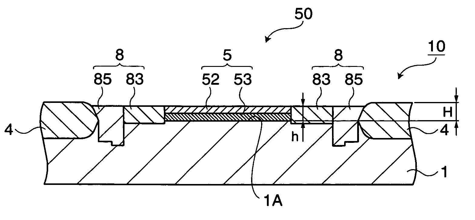
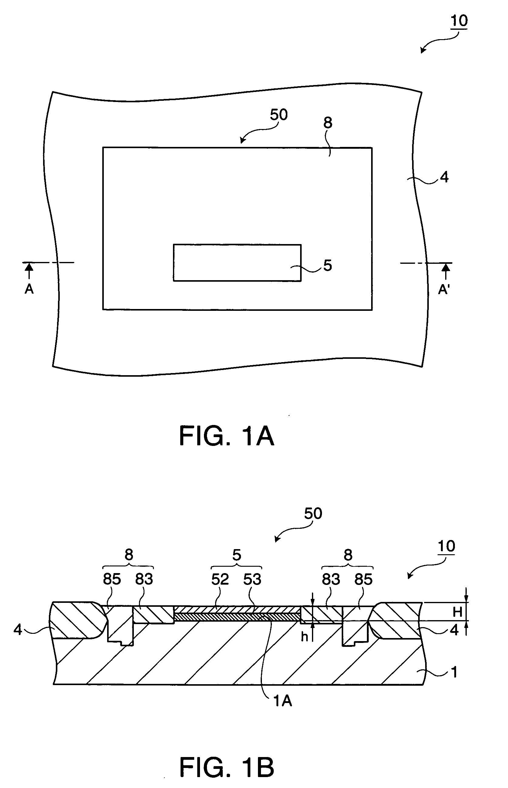
[0039]FIGS. 1A and 1B show a semiconductor substrate 10 according to a first embodiment.

[0040]FIG. 1A is a plan view schematically showing the semiconductor substrate 10 according to the embodiment while FIG. 1B is a schematic sectional view taken along a line A to A′ in FIG. 1A.

[0041]In FIGS. 1A and 1B, the semiconductor substrate 10 includes an SOI structure 5, an SOI structure region 50, and a LOCOS film 4. The SOI structure 5 is made of a silicon layer 52 and a buried insulating layer 53, and formed on an uppermost surface 1A of a bulk silicon wafer 1 serving as a semiconductor member. The SOI structure region 50 includes an insulating film 8 composed of a portion left from a support 83 used at the time of forming the SOI structure 5 and a part of a covering insulating film 85 after planarization. The SOI structure region 50 is isolated from other regions on the bulk silicon wafer 1 by the LOCOS film 4.

[0042]Then, a height H from the uppermost surface 1A of the bulk silicon wafe...

second embodiment

[0090]Next, a method for manufacturing a semiconductor device according to a second embodiment of the invention will be described.

[0091]FIGS. 15A and 15B show a semiconductor device 20 according to the second embodiment.

[0092]FIG. 15A is a schematic plan view while FIG. 15B is a schematic sectional view taken along the line A-A′ in FIG. 15A.

[0093]FIGS. 15A and 15B are schematic views showing a method for manufacturing the semiconductor device 20 according to the second embodiment of the invention.

[0094]The method for manufacturing the semiconductor device 20 includes forming a gate electrode 23 shown in FIGS. 15A and 15B following the method for manufacturing a semiconductor substrate described in FIG. 1A through 14B.

[0095]A gate insulating film that is not shown is formed on the surface of the silicon layer 52 by thermal oxidation. Then, a polysilicon film is formed on the gate insulating film by a method such as chemical vapor deposition. The polysilicon film is patterned by photo...


PUM


Abstract

A method for manufacturing a semiconductor substrate having a silicon-on-insulator (SOI) structure region isolated by a local oxidation of silicon (LOCOS) film and an SOI structure in the region includes forming the LOCOS film so as to make a height from an uppermost surface of a semiconductor member to a top surface of the LOCOS film be higher than a height from the uppermost surface of the semiconductor member to a top surface of the SOI structure, forming a silicon germanium layer and a silicon layer on the SOI structure region on the semiconductor member by epitaxial growth and forming a polysilicon film on a surface of the LOCOS film, forming a recess for a support to support the silicon layer to be a part of the SOI structure, forming the support on the semiconductor member, exposing a side of the silicon germanium layer and the silicon layer underneath the support, forming a cavity by removing the silicon germanium layer having the side exposed, forming the SOI structure by embedding an insulating layer to be buried in the cavity, planarizing a covering insulating film formed to cover an entire of a top surface of the semiconductor member by using the polysilicon film as a stopper, and exposing a top surface of the silicon layer in the SOI structure by etching.

Description

BACKGROUND[0001]1. Technical Field[0002]The present invention relates to a method for manufacturing a semiconductor substrate, a method for manufacturing a semiconductor device, and the semiconductor device. In particular, the invention relates to a technology to form a silicon-on-insulator (SOI) structure on a semiconductor substrate.[0003]2. Related Art[0004]Field effect transistors formed on an SOI structure have a huge benefit in which semiconductor devices having them can achieve low power consumption and high-speed operation. This is because the field effect transistors on the SOI structure have smaller junction capacitance, which is capacitance between a source-drain region and a substrate, compared with those formed on a bulk silicon wafer.[0005]Accordingly, a semiconductor device that can include both a transistor on a bulk silicon wafer, which is capable of operating a load requiring large power consumption, and a transistor formed on an SOI structure has been known.[0006]...

Claims


Application Information

Patent Timeline
IPC IPC(8): H01L21/84H01L21/00
CPCH01L21/76202H01L29/66772H01L21/18H01L21/20H01L21/76
Inventor KANEMOTO, KEI
Owner SEIKO EPSON CORP
Why Eureka
Try Eureka