Process for Regeneration of a Layer Transferred Wafer and Regenerated Layer Transferred Wafer

a layer transfer and regeneration technology, applied in the direction of grinding machine components, manufacturing tools, lapping machines, etc., can solve the problems of difficult use more time is required to regenerate surface roughness etc., to achieve the reduction of the processing time required for the regeneration of the layer transfer wafer, the effect of increasing the number of regeneration times and reducing the cost of the regeneration

Active Publication Date: 2007-06-28
SUMCO CORP
View PDF2 Cites 36 Cited by
  • Summary
  • Abstract
  • Description
  • Claims
  • Application Information

AI Technical Summary

Benefits of technology

[0013] According to the process for regeneration of a layer transferred wafer described in claim 1, the semiconductor wafer is separated from the thin layer on the whole surface of the ion implanted area, and no step is generated in the periphery of the separated surface of the layer transferred wafer. Therefore, the conventional chamfering or etching which has been carried out in order to remove an ion implanted layer remaining on this step can be omitted. Thus, according to the invention in claim 1, a processing time required for the regeneration of a layer transferred wafer is reduced than before, the regeneration cost is reduced and the number of regeneration times can be increased since a removal amount at regeneration is decreased.
[0014] Also, since the semiconductor wafer is formed so that the main flat portion protrudes from the chamfered portion and has the ring-shape step, an outer diameter D1 of the main flat portion becomes smaller than an outer diameter D2 of the support wafer, and the whole of the main flat portion is in contact with the support wafer, the semiconductor wafer can be separated from the thin layer on the whole surface of the ion implanted area relatively easily.
[0022] By the process for regeneration of a layer transferred wafer described in claim 5, by setting the removal amount at polishing shown in FIG. 3(c) to not more than 1 μm, a processing time required for regeneration of the layer transferred wafer is reduced to lower the regeneration cost and the number of regeneration times can be sufficiently increased. Here, if the removal amount exceeds 1 μm, there is a problem that flatness on the polished surface might be deteriorated, while if the removal amount is less than 0.2 μm, there is a problem that the damage area on the separated surface can not be removed.
[0026] By the process for regeneration of a layer transferred wafer described in claim 7, making the initial semiconductor wafer relatively thick, the regenerated wafer can be reused two times or more, which can further reduce the manufacturing cost of the SOI wafer.

Problems solved by technology

And when the semiconductor wafer is separated to be a thin film with the ion implanted area as the cleaved surface, its periphery remains not separated, and there is a problem that a step is generated in the periphery of the regenerated layer transferred wafer.
Also, a damage layer due to ion-implanting exists on the separated surface of the layer transferred wafer and the surface roughness can be large, which makes it difficult to use the layer transferred wafer as it is.
However, by the conventional process for regeneration of a layer transferred wafer shown in the patent document 1, since the ion implanted layer is removed by chamfering or etching and then subjected to mirror polishing, the surface roughness of the layer transferred wafer can be reduced, but the problem is that more time is required to regenerate the layer transferred wafer and the number of times capable of regeneration is decreased since a removal amount of a wafer to be processed is relatively increased due to grinding.

Method used


Image

  • Process for Regeneration of a Layer Transferred Wafer and Regenerated Layer Transferred Wafer
  • Process for Regeneration of a Layer Transferred Wafer and Regenerated Layer Transferred Wafer
  • Process for Regeneration of a Layer Transferred Wafer and Regenerated Layer Transferred Wafer

Examples


Embodiment Construction

[0032] Next, the preferred embodiment of the present invention will be described based on the drawings.

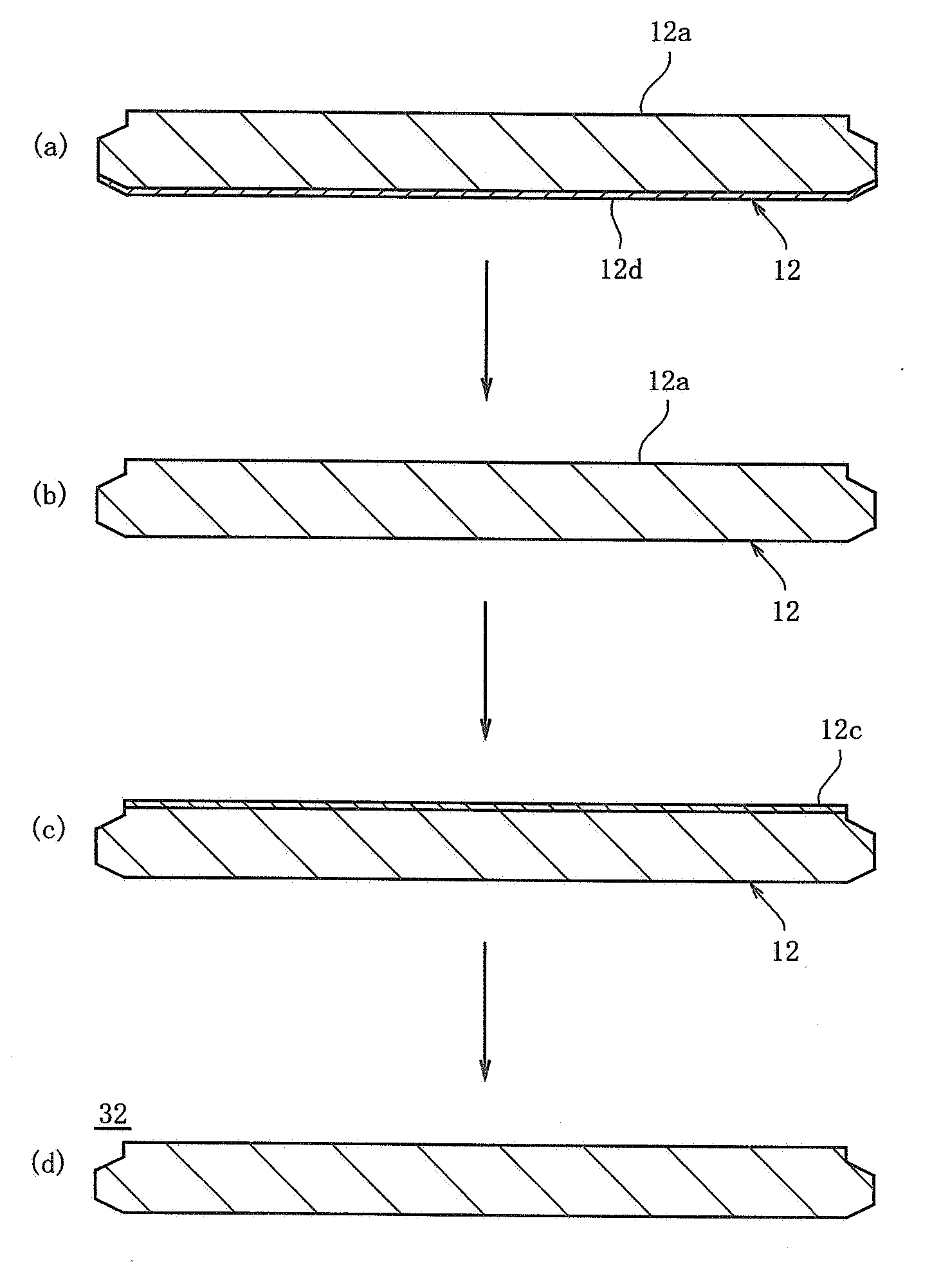
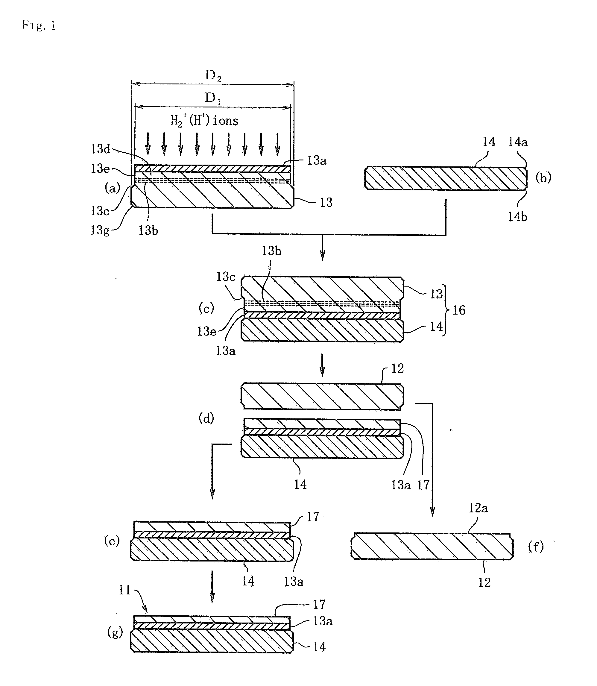
[0033] As shown in FIG. 1, a layer transferred wafer 12 is generated secondarily when producing SOI wafer 11. In order to produce the SOI wafer 11, as shown in FIG. 1(a), a semiconductor wafer 13 as a bond wafer and a support wafer 14 as a base wafer are prepared. In this preferred embodiment, these wafers 13 and 14 are produced by the Czochralski method, respectively, and they have the same diameter and the same thickness, and chamfered portions 13c, 13g, 14a and 14b are formed respectively in the periphery of both the main surfaces. These wafers 13, 14 are subjected to the RCA cleaning after polishing both the surfaces.

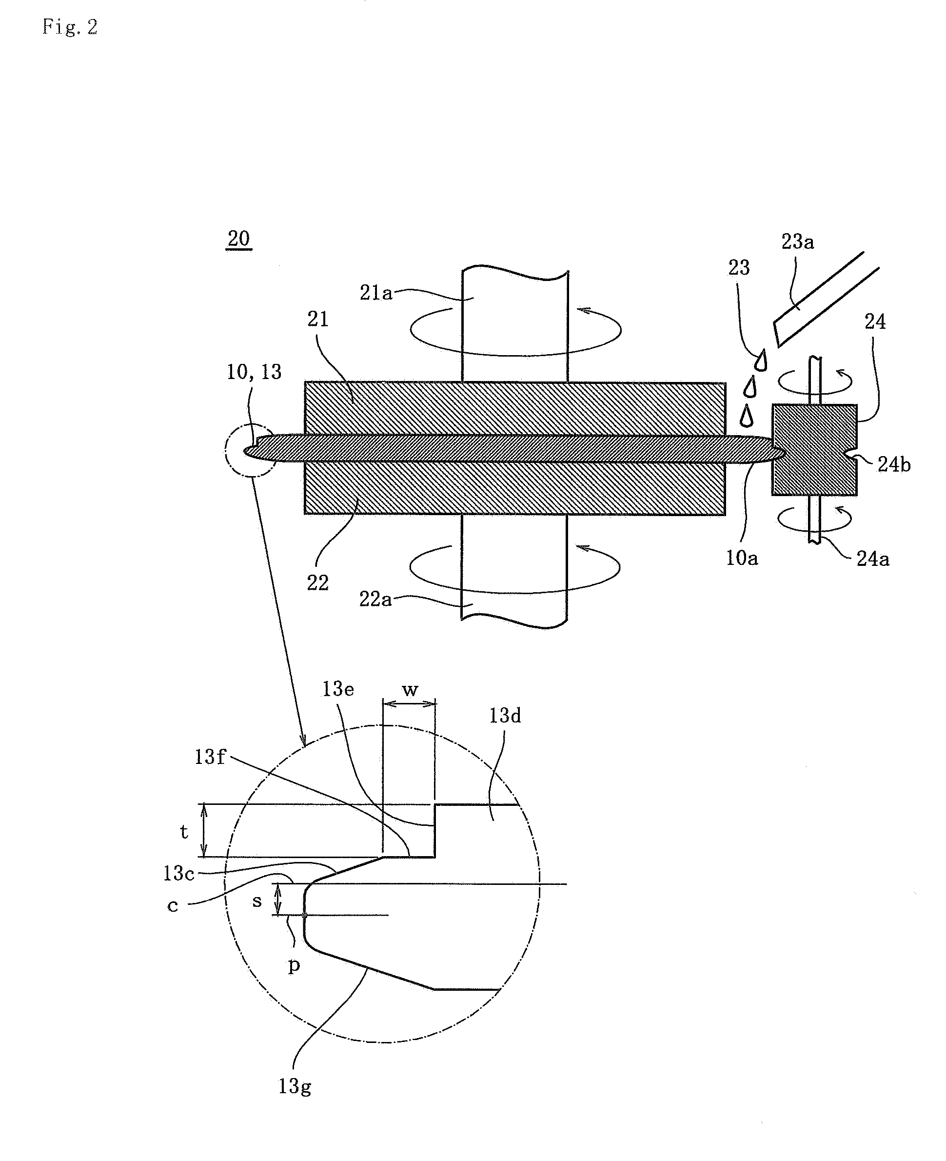
[0034] However, a main flat portion 13d is formed on one of the main surfaces of the semiconductor wafer 13, and the main flat portion 13d is formed so that it has a ring-shape step 13e on the periphery protruding from the chamfered portion 13c formed on the peri...


PUM


Abstract

A processing time required for regeneration of a layer transferred wafer is reduced and the regeneration cost is lowered, while a removal amount at the regeneration is decreased the number of regeneration times is increased. A main surface of a semiconductor wafer (13) has a main flat portion (13d) and a chamfered portion (13c) formed in the periphery of the main flat portion (13d), an ion implanted area (13b) is formed by implanting ions only into the main flat portion (13d), a laminated body (16) is formed by laminating the main flat portion (13d) on a main surface of a support wafer (14), and moreover, the semiconductor wafer (13) is separated from a thin layer (17) in the ion implanted area (13b) by heat treatment at a predetermined temperature so as to obtain a thick layer transferred wafer (12), which is to be regenerated. The main flat portion (13d) of the semiconductor wafer (13) is formed to have a ring-shape step (13e) protruding from the chamfered portion (13c), and the semiconductor wafer (13) is separated from the thin layer (17) on the whole surface of the ion implanted area (13b) so that no step is generated in the periphery thereby to obtain the layer transferred wafer (12).

Description

BACKGROUND OF THE INVENTION [0001] 1. Field of the Invention [0002] The present invention relates to a process for regeneration of a thick layer transferred wafer obtained by forming a laminated body by laminating a semiconductor wafer onto which implanted into a support wafer and by separating from a thin layer of the semiconductor wafer in the ion implanted area by heat treatment of this laminated body and a layer transferred wafer regenerated by this process. The present invention relates more particularly to a process for regeneration of a layer transferred wafer regenerated in the so-called ion implantation separation method for producing bonded wafers such as SOI (Silicon On Insulator) and a regenerated wafer. [0003] 2. Description of the Related Art [0004] As a conventional process for manufacturing an SOI wafer, a process is known in which an ion is implanted on a main surface of a semiconductor wafer to form an ion implanted area inside the semiconductor wafer, a main surfa...

Claims


Application Information

Patent Timeline
Patent Type & Authority Applications(United States)
IPC IPC(8): B24B51/00H01L21/30
CPCB24B37/042H01L21/02032H01L21/76254
Inventor MORITA, ETSUROUOKAWA, SHINJIONO, ISOROKU
Owner SUMCO CORP
Why Eureka
Try Eureka