Method for fabricating semiconductor device with bulb shaped recess gate pattern

a semiconductor device and recess gate technology, applied in the field of semiconductor device fabrication, can solve the problems of short gate channel length, high ion-implantation concentration, poor refresh property of semiconductor devices, etc., and achieve the effects of reducing abnormalities, reducing damage to the top, and increasing etch selectivity

Active Publication Date: 2007-06-28
SK HYNIX INC
View PDF14 Cites 23 Cited by
  • Summary
  • Abstract
  • Description
  • Claims
  • Application Information

AI Technical Summary

Benefits of technology

[0011] Consistent with embodiments of the present invention, there is provided a method for fabricating a semiconductor device with a bulb shaped recess gate pattern with reduced damages to a top and a side thereof and with reduced abnormality by increasing an etch selectivity between an oxide layer and silicon.

Problems solved by technology

As semiconductor devices became more highly integrated, a conventional planar type gate interconnection line including a gate pattern formed over a flat active region results in a short gate channel length and high ion-implantation concentration.
Accordingly, junction leakage is generated due to an increased electric field and thus, the semiconductor device has a poor refresh property.
During the etching process, because of a low etch selectivity ratio between silicon and an oxide layer, the substrate becomes very sensitive to a chamber condition and a surface thereof may be damaged.
As a result, the bulb shaped recess gate pattern may be unstable.

Method used


Image

  • Method for fabricating semiconductor device with bulb shaped recess gate pattern
  • Method for fabricating semiconductor device with bulb shaped recess gate pattern
  • Method for fabricating semiconductor device with bulb shaped recess gate pattern

Examples


Embodiment Construction

[0019] Hereinafter, detailed descriptions of certain embodiments consistent with the present invention will be provided with reference to the accompanying drawings.

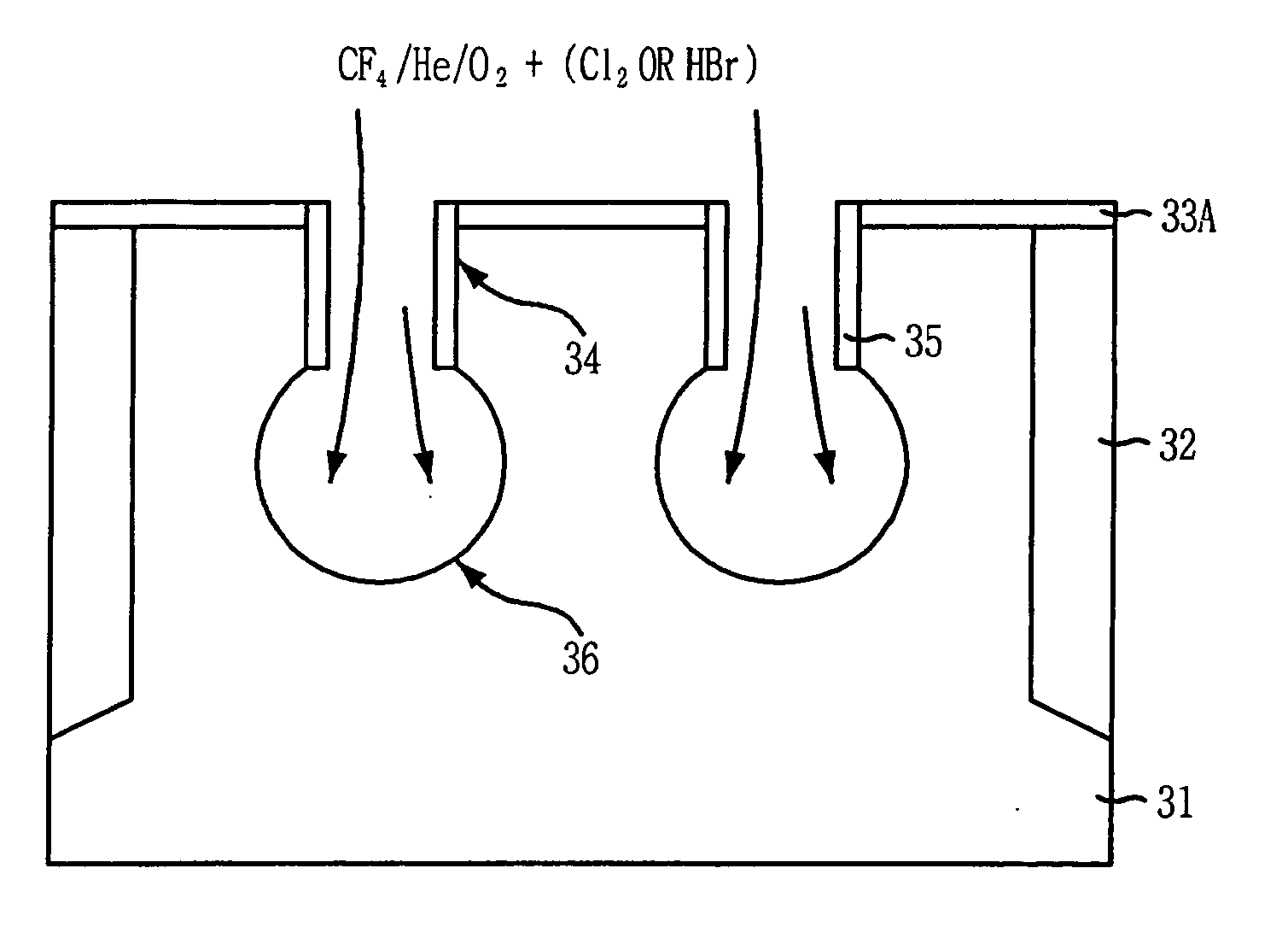
[0020]FIGS. 3A to 3E are cross-sectional views illustrating a method for fabricating a bulb shaped recess gate pattern consistent with embodiments of the present invention.

[0021] As shown in FIG. 3A, a plurality of device isolation layers 32 are formed in a substrate 31 through a shallow trench isolation (STI) process. Herein, the device isolation layers 32 are formed to define an active region and thus, the device isolation layers 32 have a greater depth than a recess gate pattern subsequently formed.

[0022] To form the device isolation layers 32, predetermined portions of the substrate 31 are etched, thereby forming trenches. Insulation layers are buried into the trenches and polished through a chemical mechanical polishing (CMP) process to form the device isolation layers 32.

[0023] Subsequently, a plurality of mask ...


PUM


Abstract

A method for fabricating a semiconductor device with a bulb shaped recess gate pattern includes selectively etching a first portion of a substrate to form a first recess; forming a spacer on sidewalls of the first recess; performing an isotropic etching process on a second portion of the substrate beneath the first recess to form a second recess, the second recess being wider and more rounded than the first recess; removing the spacer; and forming a gate pattern having a first portion buried into the first and second recesses and a second portion projecting over the substrate.

Description

RELATED APPLICATION [0001] This application is based upon and claims the benefit of priority from the prior Korean Patent Application No. 10-2005-0127736, filed Dec. 22, 2005, the entire contents of which are incorporated herein by reference. TECHNICAL FIELD [0002] The present invention relates to a method for fabricating a semiconductor device; and more particularly, to a method for fabricating a semiconductor device with a bulb shaped recess gate pattern. DESCRIPTION OF RELATED ARTS [0003] As semiconductor devices became more highly integrated, a conventional planar type gate interconnection line including a gate pattern formed over a flat active region results in a short gate channel length and high ion-implantation concentration. Accordingly, junction leakage is generated due to an increased electric field and thus, the semiconductor device has a poor refresh property. [0004] To alleviate the above problem associated with a conventional planar type gate interconnection line, a p...

Claims


Application Information

Patent Timeline
Patent Type & Authority Applications(United States)
IPC IPC(8): H01L21/3205
CPCH01L21/3065H01L29/66621H01L21/18
Inventor CHO, YONG-TAEKIM, SUK-KI
Owner SK HYNIX INC
Why Eureka
Try Eureka