CMOS image sensor with backside illumination and method for manufacturing the same

a technology of image sensor and backside illumination, which is applied in the field of image sensor, can solve the problems of deteriorating sensitivity of cmos image sensor, reducing the quantity of light incident, and complicated overall process, and achieves the effect of easy realization of color images

Active Publication Date: 2007-07-05
INTELLECTUAL VENTURES II
View PDF3 Cites 64 Cited by
  • Summary
  • Abstract
  • Description
  • Claims
  • Application Information

AI Technical Summary

Benefits of technology

[0017] Embodiments of the present invention provide a complementary metal oxide semiconductor (CMOS) image sensor that can easily realize a color image by removing color filters and adjusting a backside thickness of a wafer, and a method for manufacturing the same.

Problems solved by technology

This reduction of the pixel size leads to the decrease of the quantity of light incident on the photodiode, which makes sensitivity of the CMOS image sensor to be deteriorated.
Accordingly, an overall process is too complicated.
Thus, to manufacture the CMOS image sensor with the backside illumination, multi-step processes are required, and thus the fabrication process becomes too complicated.
Although the grinding and chemical-etching processes are performed, it is somewhat difficult to obtain the wafer of which the backside has a desired thickness.
Thus, there is a limitation to realize a desired image according to the typical CMOS image sensor.

Method used


Image

  • CMOS image sensor with backside illumination and method for manufacturing the same
  • CMOS image sensor with backside illumination and method for manufacturing the same
  • CMOS image sensor with backside illumination and method for manufacturing the same

Examples


Embodiment Construction

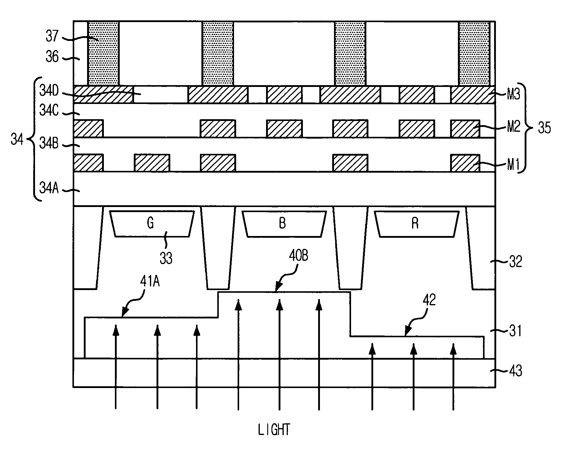
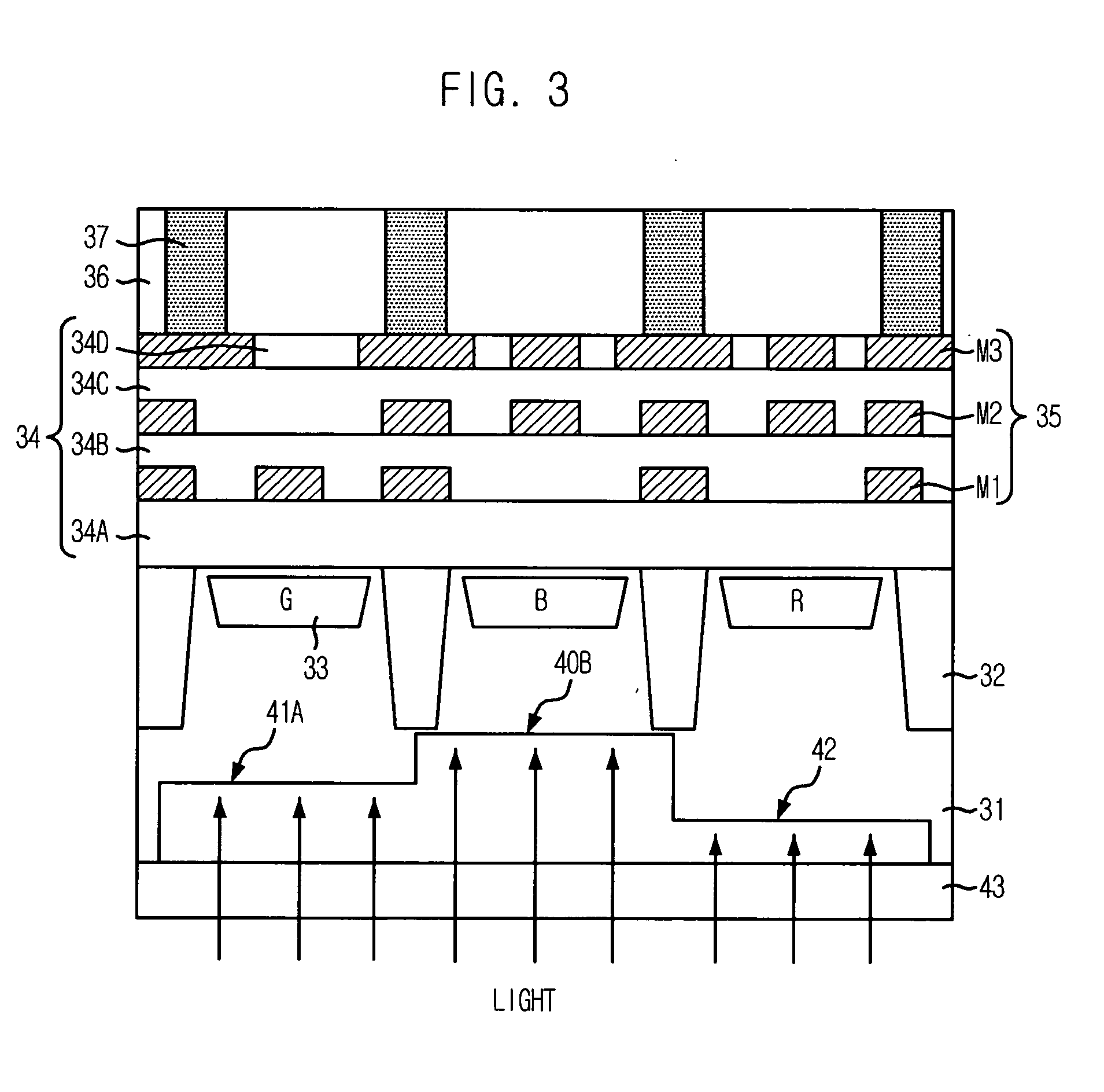
[0024]FIG. 3 illustrates a sectional view of a CMOS image sensor in accordance with an embodiment of the present invention.

[0025] Referring to FIG. 3, the CMOS image sensor in accordance with the embodiment of the present invention includes a plurality of pixel regions 33, a multi-layered metal interconnection 35, a bump 37, a first trench 40B, a second trench 41A, a third trench 42, and a glass 43. Herein, the plurality of pixel regions 33 are formed under a front surface of a substrate 31 (e.g., silicon substrate) for realizing color image, and have photodiodes separated from each other by a field oxide 32. The multi-layered metal interconnection 35 is formed over the pixel regions 33 of the front of the substrate 31. The bump 37 is connected to an uppermost metal interconnection M3 of the multi-layered metal interconnection 35. The first, second and third trenches 40B, 41A and 42 having different depths for each wavelength of light are formed in a backside of the substrate 31, a...


PUM


Abstract

A CMOS image sensor includes a plurality of pixel regions formed under a front surface of a substrate, and having photodiodes separated from each other by a field oxide, a multi-layered metal interconnection formed over the pixel regions of the front of the substrate, a bump connected to an uppermost metal interconnection of the multi-layered metal interconnection, a plurality of trenches formed in a backside of the substrate, wherein the trenches have different depths for each wavelength of light, and correspond to the respective pixel regions, and a glass covering the backside of the substrate.

Description

CROSS-REFERENCE TO RELATED APPLICATIONS [0001] The present invention claims priority of Korean patent application number 10-2005-0134110, filed on Dec. 29, 2006, which is incorporated by reference in its entirety. BACKGROUND OF THE INVENTION [0002] The present invention relates to an image sensor, and more particularly, to a complementary metal oxide semiconductor (CMOS) image sensor and a method for manufacturing the same. [0003] In general, an image sensor is a semiconductor device that converts an optical image into an electrical signal. Among the image sensors, a charge-coupled device (CCD) has a structure in which each MOS capacitor is closely located and charges are stored in the MOS capacitor and transferred. Whereas, a CMOS image sensor employs CMOS technology that uses a control circuit and a signal processing circuit as peripheral circuits and adopts a switching mode that detects outputs sequentially. Here, MOS transistors are formed in the peripheral circuit as the same n...

Claims


Application Information

Patent Timeline
Patent Type & Authority Applications(United States)
IPC IPC(8): H01L31/113H01L27/146H04N5/335H04N5/369H04N5/374
CPCH01L27/14603H01L27/14609H01L27/1464H01L27/14683H01L27/14643H01L27/146
Inventor KIM, HEE-JEEN
Owner INTELLECTUAL VENTURES II
Why Eureka
Try Eureka