Dry etch stop process for eliminating electrical shorting in MRAM device structures

Active Publication Date: 2007-07-05
OEM GRP LLC
View PDF18 Cites 23 Cited by
  • Summary
  • Abstract
  • Description
  • Claims
  • Application Information

AI Technical Summary

Benefits of technology

[0029] Also shown in FIG. 1 is a hard mask layer 24, an antireflective coating 26, and a patterned layer of photoresist 28. Photoresist layer 28 is a light sensitive material that is commonly used by those skilled in the art of electrical device fabrication as a mask to etch one or more of the underlying layers below the photoresist so that portions of the underlying layer not protected by the resist layer can be etched away. Antireflection coating 26, which is typically 300 Å to 800 Å thick, is commonly used to absorb radiation to form an optically opaque film to enhance the contrast of the imaging resist. ARC coatings effectively reduce reflection of the incident radiation back into the overlying PR m

Problems solved by technology

Ion beam milling operates with low selectivity, and the portions of the stack that are near to the edges of the mask or the boundaries of an MRAM cell body can be easily damaged.
One of the drawbacks of current etching techniques is that the profiles of MRAM structures ar

Method used


Image

  • Dry etch stop process for eliminating electrical shorting in MRAM device structures
  • Dry etch stop process for eliminating electrical shorting in MRAM device structures
  • Dry etch stop process for eliminating electrical shorting in MRAM device structures

Examples


Example

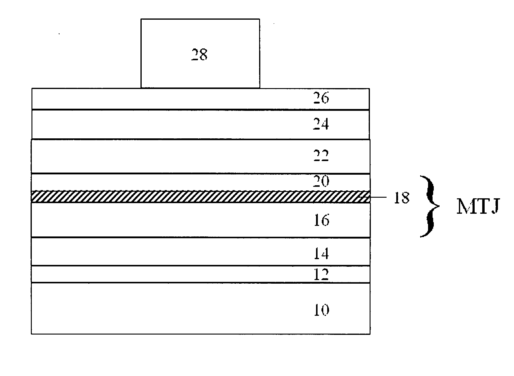
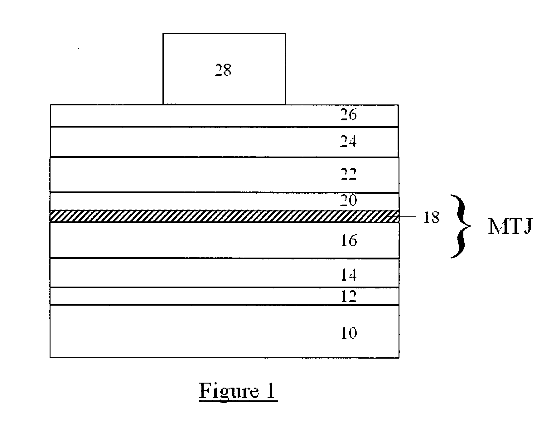
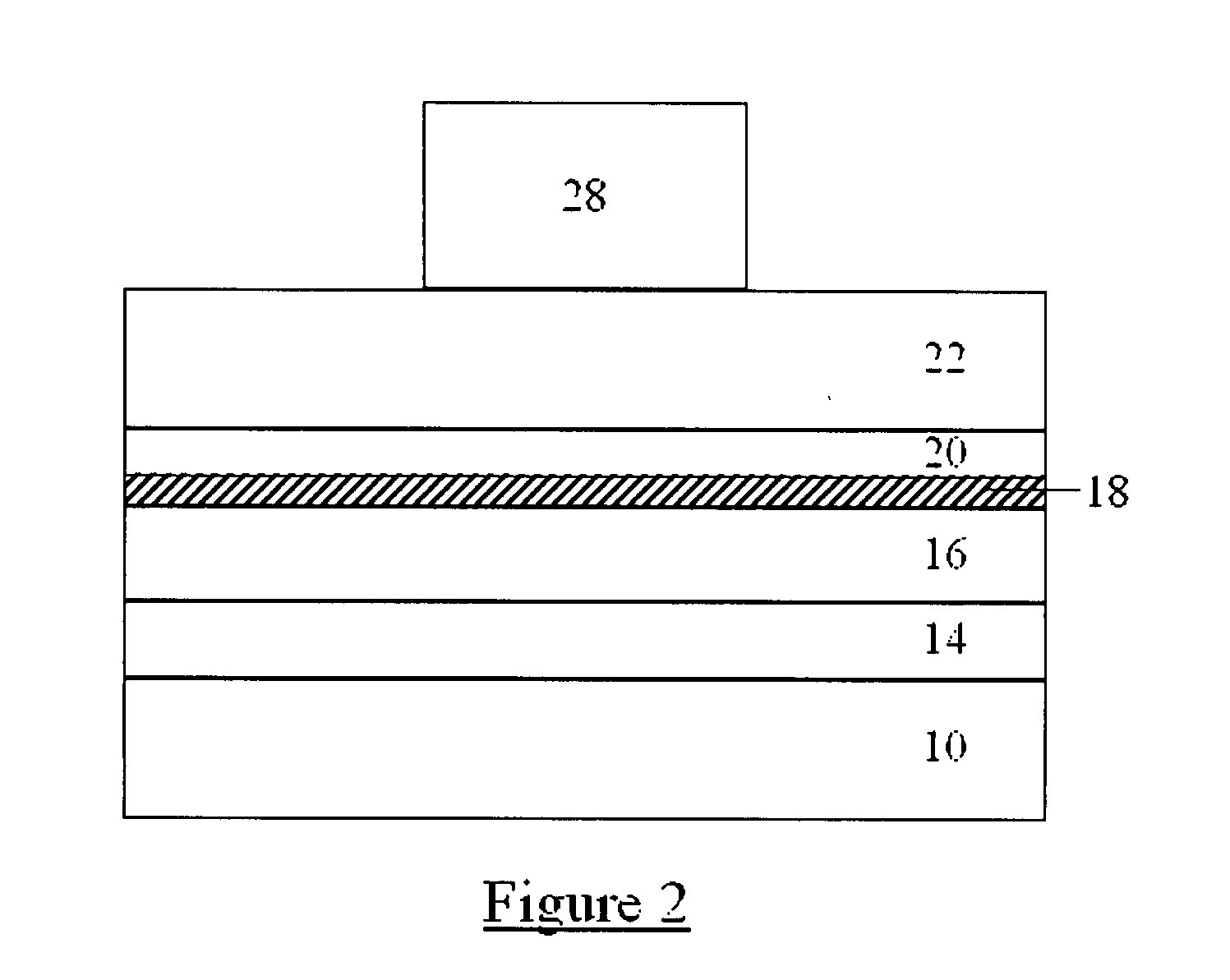
[0027] The present invention is based, in part, on the development of a patterning method for fabricating magnetic tunnel junction (MTJ) devices that are employed in magnetic random access memory (MRAM) devices. As further described herein, a critical aspect of the invention is that MTJ devices prepared by the inventive process afford superior electrical isolation between the magnet layers in contact with the dielectric tunnel layer in comparison to the current art.

[0028] A typical MRAM structure, within which an MTJ is contained, is shown in FIG. 1. The MRAM structure is a complex stack of magnetic, conductive, and insulating films on a substrate. In FIG. 1, the specific components of a typical MRAM structure are shown and consist of a substrate 10, a barrier layer 12, a bottom contact layer 14, a mulitlayer fixed magnet structure 16 consisting of layers of CoFe, Ru, NiFe, IrMn, PtMn, and the like, a dielectric tunnel layer such as alumina or MgO 18, a switchable magnet layer 20 (...


PUM


Abstract

The present invention relates generally to semiconductor fabrication and particularly to fabricating magnetic tunnel junction devices. In particular, this invention relates to a method for using the dielectric layer in tunnel junctions as an etch stop layer to eliminate electrical shorting that can result from the patterning process.

Description

[0001] This application claims priority from U.S. provisional applications Ser. No. 60 / 783,157, filed Mar. 16, 2005, entitled “Dry etch stop process for eliminating electrical shorting in MRAM device structures”, which is incorporated herein by reference.FIELD OF THE INVENTION [0002] The present invention relates generally to semiconductor fabrication and particularly to fabricating device structures containing metal-insulator-metal layered thin film stacks such as those used in magnetic tunnel junction devices and memory devices. BACKGROUND OF THE INVENTION [0003] Layered films of metal-insulator-metal are employed as storage elements in memory devices such as magnetic random access memories (MRAM) and the like. The memory element for the MRAM technology is a patterned structure of multilayer material and is usually composed of a stack of different materials such as NiFe, CoFe, PtMn, Ru, etc., and may include insulator-like materials such as Al203 or MgO. A typical stack may contai...

Claims


Application Information

Patent Timeline
IPC IPC(8): H01L21/00
CPCH01L43/12H10N50/01
Inventor DITIZIO, ROBERT ANTHONY
Owner OEM GRP LLC
Why Eureka
Try Eureka