Excessive round-hole shielded gate trench (SGT) MOSFET devices and manufacturing processes

Active Publication Date: 2007-07-12
ALPHA & OMEGA SEMICON LTD
View PDF1 Cites 23 Cited by
  • Summary
  • Abstract
  • Description
  • Claims
  • Application Information

AI Technical Summary

Benefits of technology

[0008] It is therefore an object of the present invention to provide a new and improved semiconductor power device implemented with the shielded gate trench (SGT) structure that opened as a round hole with lateral expansion beyond the trench walls to provide as landmark of vertical alignment. The depth of the trenched gate can be accurately controlled with the lateral expansion as vertical alignment such that the gate to drain capacitance can be accurately manufactured to overcome the above discussed technical difficulties and limitations.
[0009] Specifically, it is an object of the present invention to provide improved device configuration and manufacturing method to reduce the gate to drain capacitance while accurately control the device parameters including the gate to drain capacitance by controlling the depth of the trenched gate. The depth of the trenched gate is controlled by forming a round hole SGT structure with lateral expansion from the trenches such that the depth of the trenched gate is accurately controlled by a time etch using the round hole lateral expansion as a control indication for vertical alignme

Problems solved by technology

Conventional technologies for reducing the gate to drain capacitance Cgd in a DMOS device by employing the shielded gate trench (SGT) structure are still confronted with technical limitations and difficulties.
A carefully controlled time etch is carried out to control the depth D. However, the depth of the trench bottom D cannot be accurately controlled due to the variations of the etch speed of the polysilicon from the top portion of the trenches.
As described above, even with accurate time control of an etch process, the depth of the polysilicon gate relative to the top surface of the

Method used


Image

  • Excessive round-hole shielded gate trench (SGT) MOSFET devices and manufacturing processes
  • Excessive round-hole shielded gate trench (SGT) MOSFET devices and manufacturing processes
  • Excessive round-hole shielded gate trench (SGT) MOSFET devices and manufacturing processes

Examples


Example

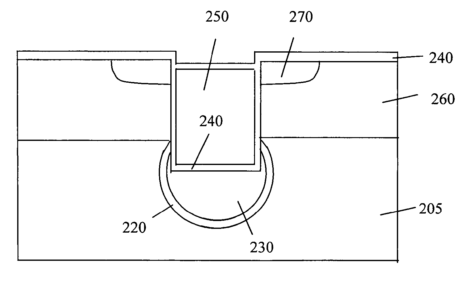
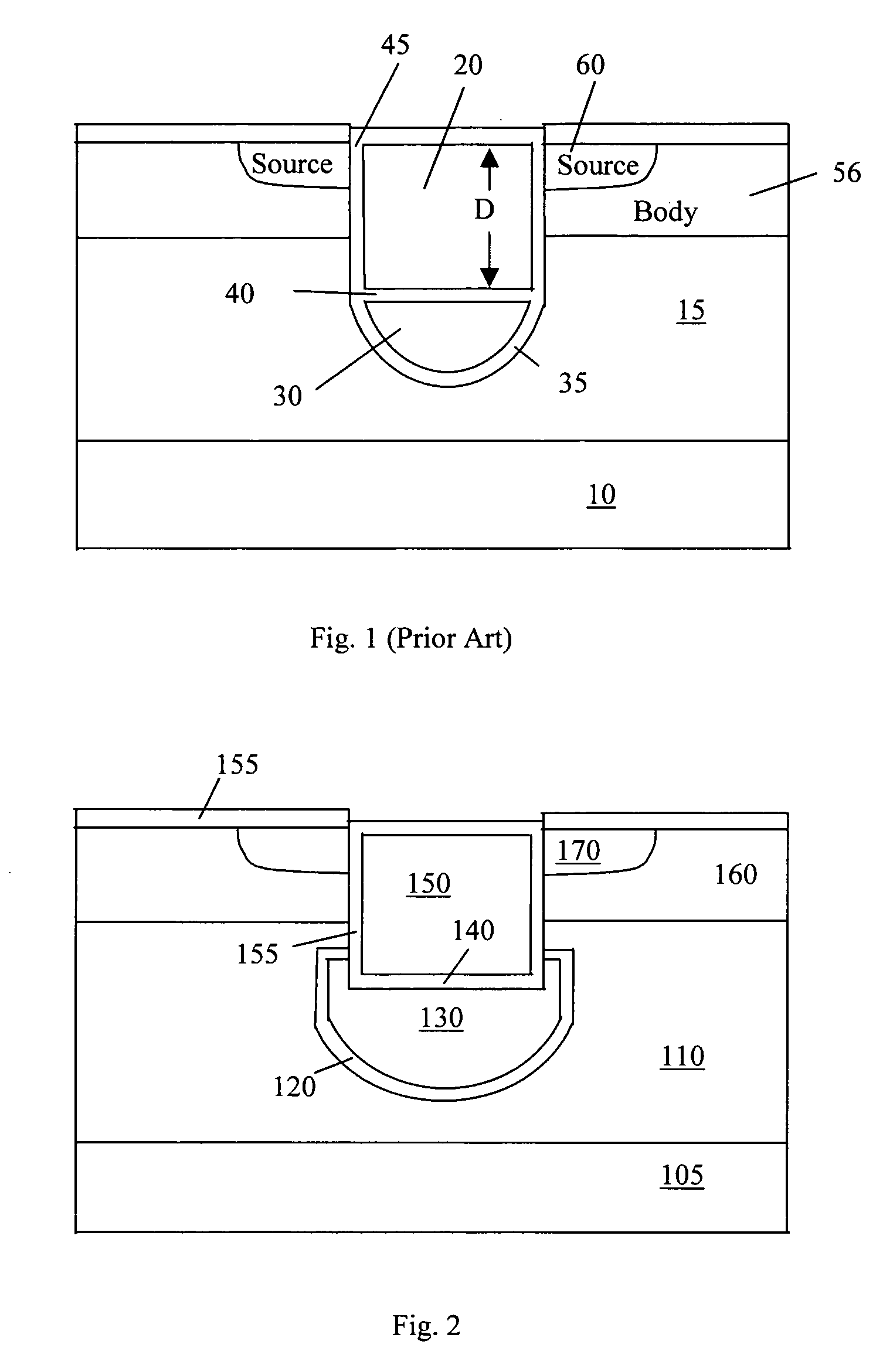
[0015] Referring to FIG. 2 for a cross sectional view of a trenched MOSFET device 100 of this invention. The trenched MOSFET device 100 is supported on a substrate 105 formed with an epitaxial layer 110. The trenched MOSFET device 100 includes a shielded gate trench (SGT) structure 130 opened as a round hole shielding structure below a trenched gate 150. The round hole SGT structure 130 filled with a polysilicon therein is provided to shield and insulate the trenched gate 150 from the drain disposed below the drain 105 by insulation layers 120 surrounding the SGT structure 130 and the oxide layer 140 between the SGT structure 130 and the trenched gate 150. The trenched gate 150 includes polysilicon filling in a trench surrounded with a gate insulation layer 155 covering the trenched walls. A body region 160 that is doped with a dopant of second conductivity type, e.g., P-type dopant, extends between the trenched gates 150. The P-body regions 160 encompassing a source region 170 dope...


PUM


Abstract

This invention discloses an improved trenched metal oxide semiconductor field effect transistor (MOSFET) device that includes a trenched gate surrounded by a source region encompassed in a body region above a drain region disposed on a bottom surface of a substrate. The MOSFET cell further includes a shielded gate trench (SGT) structure below and insulated from the trenched gate. The SGT structure is formed substantially as a round hole having a lateral expansion extended beyond the trench gate and covered by a dielectric linen layer filled with a trenched gate material. The round hole is formed by an isotropic etch at the bottom of the trenched gate and is insulated from the trenched gate by an oxide insulation layer. The round hole has a lateral expansion beyond the trench walls and the lateral expansion serves as a vertical alignment landmark for controlling the depth of the trenched gate. The MOSFET device has a reduced gate to drain capacitance Cgd depending on the controllable depth of the trenched gate disposed above the SGT structure formed as a round hole below the trenched gate.

Description

BACKGROUND OF THE INVENTION [0001] 1. Field of the Invention [0002] The invention relates generally to the semiconductor power devices. More particularly, this invention relates to an improved and novel manufacturing process and device configuration for providing the shielded trench gates having precisely controllable depth below the silicon top surface such that the reduction of gate to drain capacitance can be accurately achieved. [0003] 2. Description of the Prior Art [0004] Conventional technologies for reducing the gate to drain capacitance Cgd in a DMOS device by employing the shielded gate trench (SGT) structure are still confronted with technical limitations and difficulties. Specifically, trenched DMOS devices are configured with trenched gates wherein large capacitance (Cgd) between gate and drain limits the device switching speed. The capacitance is mainly generated from the electrical field coupling between the bottom of the trenched gate and the drain. In order to reduc...

Claims


Application Information

Patent Timeline
IPC IPC(8): H01L29/76H01L29/94H01L31/00
CPCH01L21/76232H01L29/4236H01L29/7834H01L29/66621H01L29/42376
Inventor CHANG, HONGTAI, SUNG-SHANLI, TIESHENGWANG, YU
Owner ALPHA & OMEGA SEMICON LTD
Why Eureka
Try Eureka