

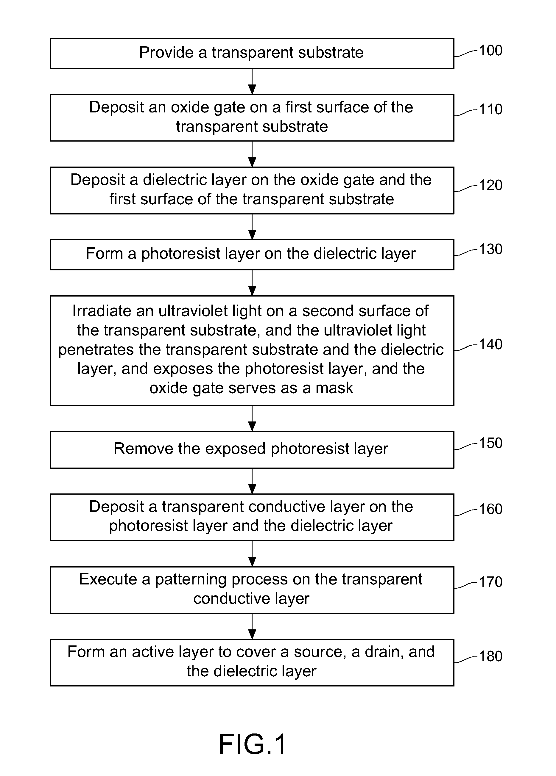
Method for manufacturing self-aligned thin-film transistor and structure thereof
- Summary
- Abstract
- Description
- Claims
- Application Information
AI Technical Summary
Benefits of technology
Problems solved by technology
Method used
Image

Examples
first embodiment
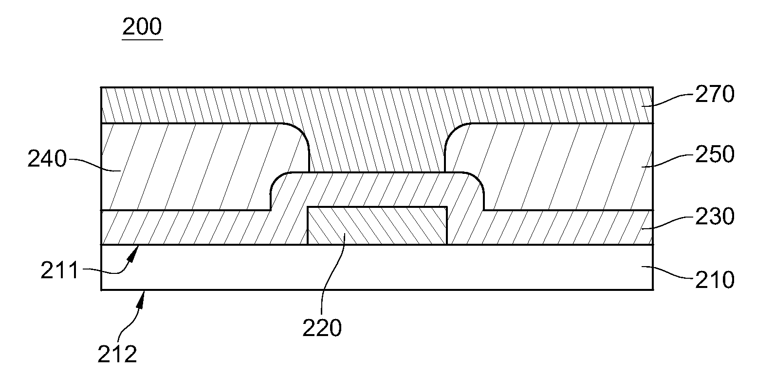
[0027]Through the above steps, the TFT 200 of a bottom gate type according to the present invention as shown in FIG. 2F is finished. The TFT 200 comprises the transparent substrate 210, and the oxide gate 220, the dielectric layer 230, the source 240, the drain 250, and the active layer 270 disposed on the transparent substrate 210 in sequence.
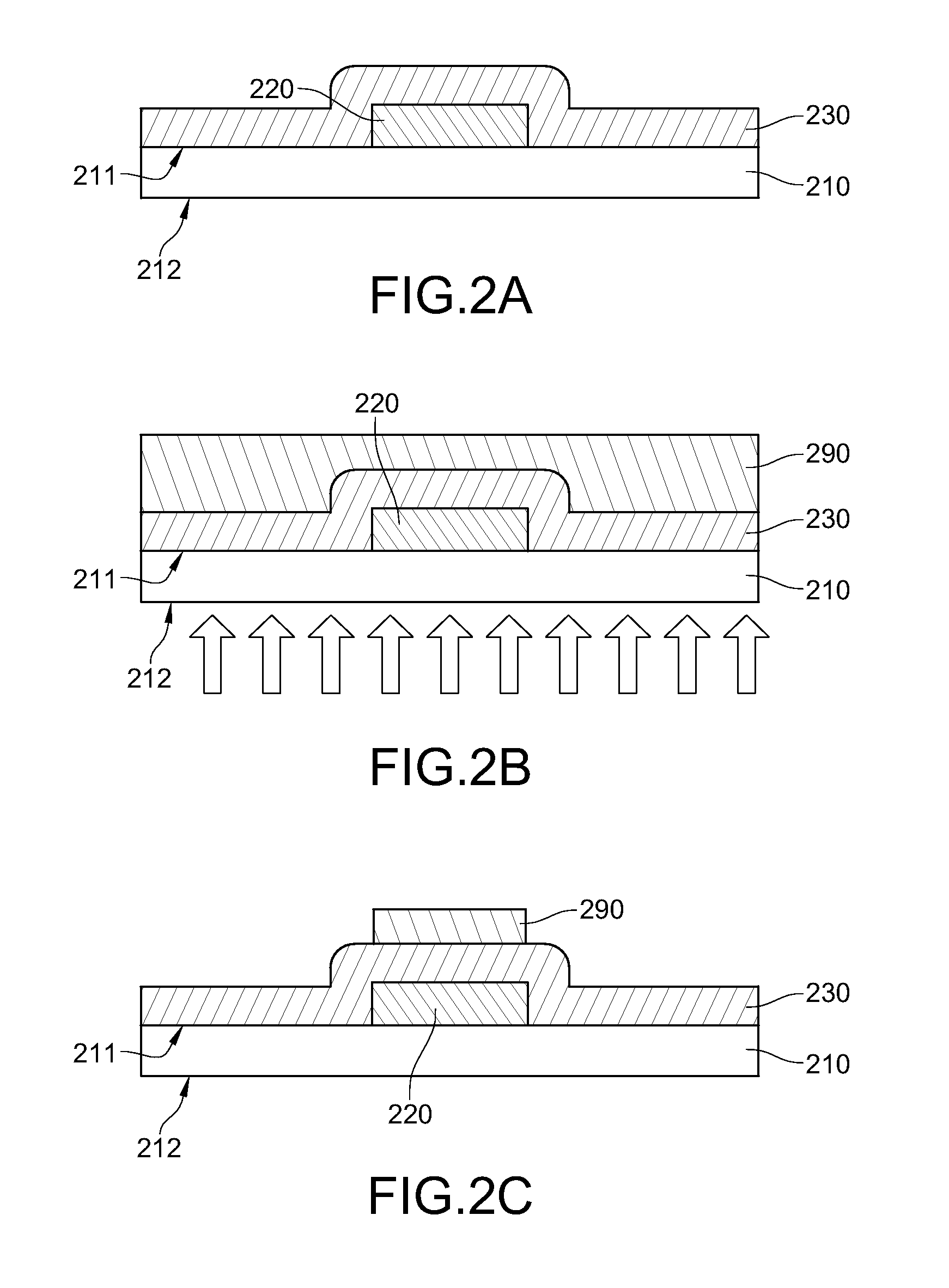
[0028]FIG. 4 and FIGS. 5A to 5G are respectively a flow chart of steps and schematic views of detailed steps according to a second embodiment of the present invention. Referring to FIG. 5A and the descriptions of the steps of FIG. 4, in a method for manufacturing a self-aligned TFT according to the second embodiment of the present invention, firstly, a transparent substrate 210 is provided (Step 100), in which the transparent substrate 210 has a first surface 211 and a second surface 212 opposite to each other (that is, respectively a top surface and a bottom surface of the transparent substrate 210). The transparent substrate 210 according to...
second embodiment
[0034]Through the above steps, the TFT 200 of a bottom gate type according to the present invention as shown in FIG. 5G is finished. The TFT 200 includes the transparent substrate 210, and the oxide gate 220, the dielectric layer 230, the source 240, the drain 250, and the active layer 270 disposed on the transparent substrate 210 in sequence.
[0035]In the method for manufacturing the self-aligned TFT and the structure thereof according to the present invention, the oxide gate serves as a bottom gate and a mask. The oxide gate has a high absorbing characteristic for the ultraviolet light, so as to shield the ultraviolet light irradiated on the photoresist layer corresponding to the oxide gate. Thus, the source and the drain are accurately manufactured in a self-aligned manner during the subsequent steps, without any deviation on the disposition positions thereof, and accordingly, the steps for manufacturing the TFT are greatly simplified.
[0036]Furthermore, the oxide gate according to...
PUM
 Abstract
Description
Claims
Application Information