Methods and semiconductor structures for latch-up suppression using a buried conductive region

Inactive Publication Date: 2007-07-12
IBM CORP
View PDF86 Cites 24 Cited by
  • Summary
  • Abstract
  • Description
  • Claims
  • Application Information

AI Technical Summary

Benefits of technology

[0011] The present invention is generally directed to semiconductor structures and methods that suppress latch-up in standard bulk CMOS device designs, while retaining cost effectiveness for integration into the process flow forming the P-channel and N-channel field effect transistors characteristic of bulk CMOS devices.

Problems solved by technology

Latch-up, which is precipitated by unwanted transistor action of parasitic bipolar transistors inherently present in bulk CMOS devices, may be a significant issue for bulk CMOS technologies.
The unwanted parasitic transistor action, which has various triggers, may cause the bulk CMOS device to fail.
Because the integrated circuit cannot be easily replaced in space-based platforms, the chip failure may prove catastrophic.
However, epitaxial substrates are expensive to produce and may increase the design complexity of several critical circuits, such as electrostatic discharge (ESD) protective devices.
Guard ring diffusions are costly because they occupy a significant amount of active area silicon real estate.
However, CMOS devices are expensive to fabricate using an SOI substrate, as compared to fabrication using bulk substrates.
Furthermore, SOI substrates suffer from various other radiation-induced failure mechanisms aside from latch-up.
Another disadvantage is that SOI devices do not generally come with a suite of ASIC books that would enable simple assembly of low-cost designs.
Conventional CMOS devices are susceptible to latch-up generally because of the close proximity of N-channel and P-channel devices.
This results in negative differential resistance behavior and, eventually, latch-up of the bulk CMOS device.
The low-impedance state may precipitate catastrophic failure of that portion of the integrated circuit.
Unfortunately, irreversible damage to the integrated circuit may occur almost instantaneously with the onset of the disturbance so that any reaction to exit the latched state is belated.

Method used


Image

  • Methods and semiconductor structures for latch-up suppression using a buried conductive region
  • Methods and semiconductor structures for latch-up suppression using a buried conductive region
  • Methods and semiconductor structures for latch-up suppression using a buried conductive region

Examples


Embodiment Construction

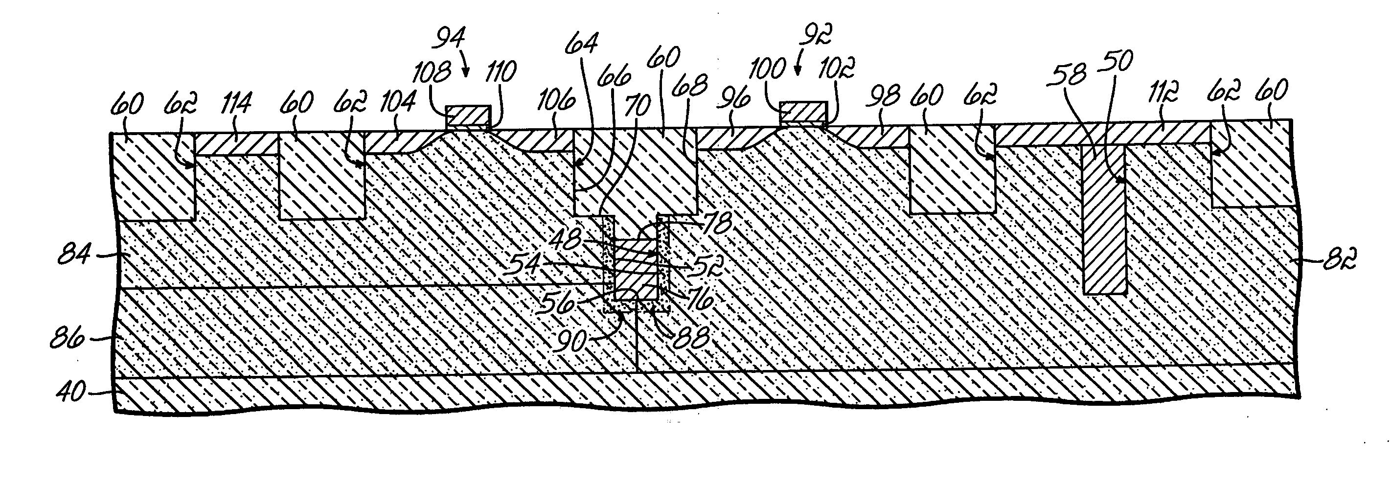
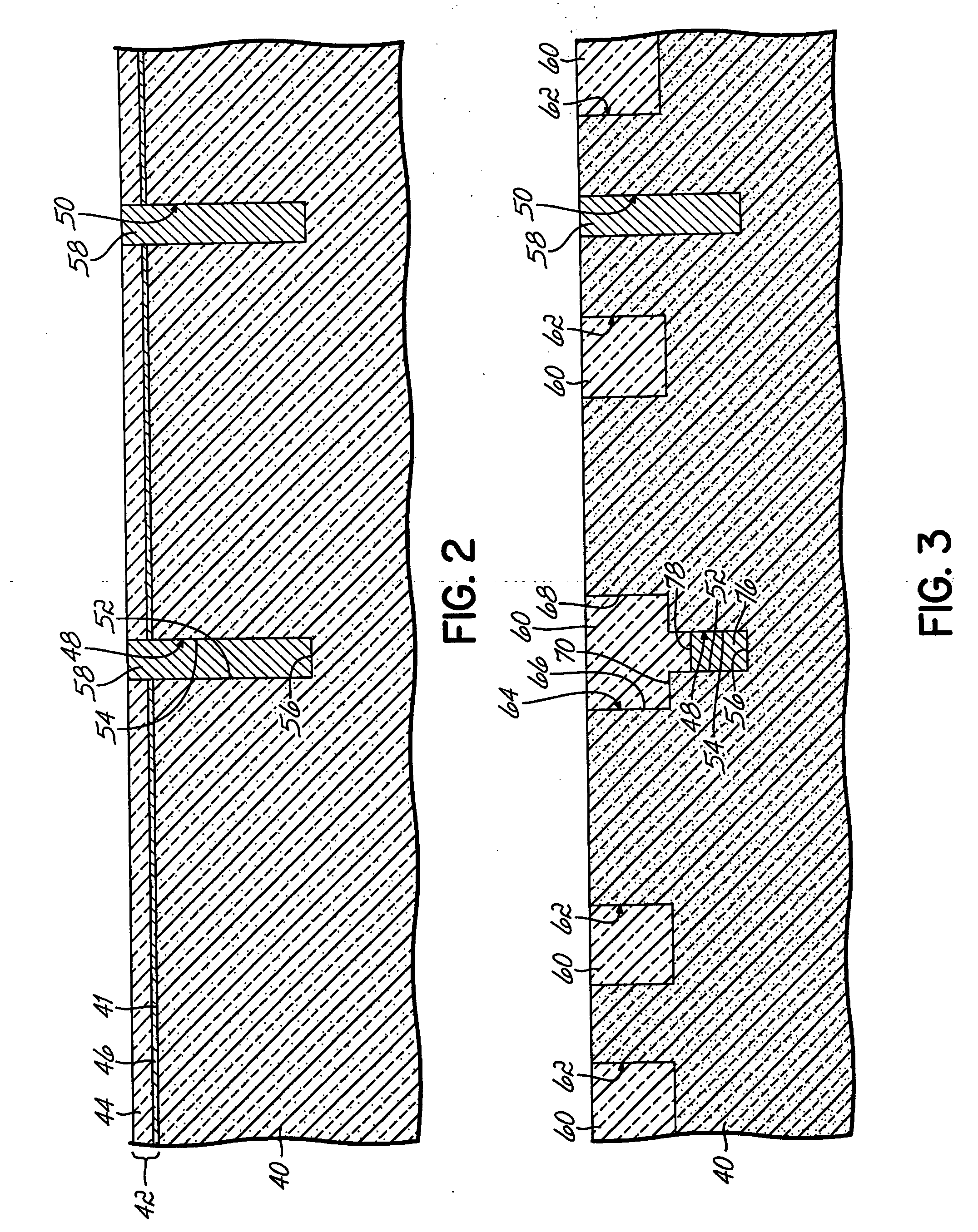
[0021] The present invention provides a buried guard region that limits the effect of the vertical parasitic NPN structure and the lateral parasitic PNP structure responsible for latch-up in triple-well bulk complementary metal-oxide-semiconductor (CMOS) devices. The invention is advantageously implemented in the context of bulk CMOS devices in which pairs of N-channel and P-channel field effect transistors are formed adjacent to each other in a P-well within an N-band and an N-well, respectively, and the P-well is isolated from the N-well by a shallow trench isolation (STI) region. Specifically, latch-up in a standard bulk CMOS triple well structure is suppressed by the addition of a heavily doped n-type region (i.e., N-well strap) diffused into the semiconductor material bordering a deep vertical extension of the trench in which the STI region is formed. The N-well strap bridges the N-well and the N-band and has a higher dopant concentration than either the N-well or the N-band. C...


PUM


Abstract

Semiconductor structures and methods for suppressing latch-up in bulk CMOS devices. The structure comprises a first doped well formed in a substrate of semiconductor material, a second doped well formed in the substrate proximate to the first doped well, and a deep trench defined in the substrate. The deep trench includes sidewalls positioned between the first and second doped wells. A buried conductive region is defined in the semiconductor material bordering the base and the sidewalls of the deep trench. The buried conductive region intersects the first and second doped wells. The buried conductive region has a higher dopant concentration than the first and second doped wells. The buried conductive region may be formed by solid phase diffusion from a mobile dopant-containing material placed in the deep trench. After the buried conductive region is formed, the mobile dopant-containing material may optionally remain in the deep trench.

Description

FIELD OF THE INVENTION [0001] The invention relates generally to semiconductor structures and methods and, in particular, to methods for reducing latch-up in bulk complementary metal-oxide-semiconductor device structures and semiconductor structures produced by these methods. BACKGROUND OF THE INVENTION [0002] Complementary metal-oxide-semiconductor (CMOS) technologies integrate P-and N-channel field effect transistors (FETs) to form an integrated circuit using a semiconductor substrate. Latch-up, which is precipitated by unwanted transistor action of parasitic bipolar transistors inherently present in bulk CMOS devices, may be a significant issue for bulk CMOS technologies. The unwanted parasitic transistor action, which has various triggers, may cause the bulk CMOS device to fail. For outer space based applications, latch-up may be induced by the impingement of high energy ionizing radiation and particles (e.g., cosmic rays, neutrons, protons, alpha particles). Because the integra...

Claims


Application Information

Patent Timeline
IPC IPC(8): H01L29/76
CPCH01L27/0921H01L21/823878
Inventor CHANG, SHUNHUA THOMASFURUKAWA, TOSHIHARUGAUTHIER, ROBERT J. JR.HORAK, DAVID VACLAVKOBURGER, CHARLES WILLIAM IIIMANDELMAN, JACK ALLANTONTI, WILLIAM ROBERT
Owner IBM CORP
Why Eureka
Try Eureka