Stratified photodiode for high resolution CMOS image sensor implemented with STI technology

Active Publication Date: 2007-07-12
INTELLECTUAL VENTURES II
View PDF8 Cites 32 Cited by
  • Summary
  • Abstract
  • Description
  • Claims
  • Application Information

AI Technical Summary

Benefits of technology

[0013] It is, therefore, an object of the present invention to provide a photodiode with a stratified doping arrangement, which allows formation of multiple junction capacitances in a photodiode re

Problems solved by technology

However, when the pinned voltage Vpin is low, it is difficult to store enough charge in the photodiode, because there is a certain practical limit to the value of the capacitance CS 105 that can be achieved.
This result is a consequence of some material limitations of silicon and some limitation in processing.
This number is difficult to achieve for sensors with pixel sizes on the order of 2.0 μm and smaller,

Method used


Image

  • Stratified photodiode for high resolution CMOS image sensor implemented with STI technology
  • Stratified photodiode for high resolution CMOS image sensor implemented with STI technology
  • Stratified photodiode for high resolution CMOS image sensor implemented with STI technology

Examples


Example

[0022] Exemplary embodiments of the present invention on a stratified photodiode for high resolution CMOS image sensor implemented with STI technology will be described in detail with reference to the accompanying drawings.

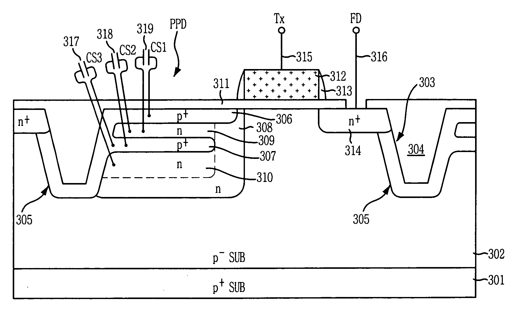
[0023]FIG. 3 is a simplified cross-sectional view illustrating a pixel structure of a CMOS image sensor with a pinned photodiode, which is constructed based on a stratified doping arrangement, in accordance with an embodiment of the present invention. In the pinned photodiode, multiple pn junction capacitances are formed since an intermediate p-type doping region is not fully depleted when a bias is applied.

[0024] Referring to FIG. 3, the CMOS image sensor pixel includes: a semi-conductive layer 302 formed over a highly doped p+-type substrate 301 (hereinafter referred to as “substrate”); an STI region 304 formed regionally in the semi-conductive layer 302; a pinned photodiode PPD formed in the semi-conductive layer 302; and a transfer gate 312 to transfer photo...


PUM


Abstract

A stratified photodiode for high resolution CMOS image sensors implemented with STI technology is provided. The photodiode includes a semi-conductive layer of a first conductivity type, multiple doping regions of a second conductivity type, multiple doping regions of the first conductivity type, and a pinning layer. The multiple doping regions of the second conductivity type are formed to different depths in the semi-conductive layer. The multiple doping regions of the first conductivity type are disposed between the multiple doping regions of the second conductivity type and form multiple junction capacitances without full depletion. In particular, the stratified doping arrangement allows the photodiode to have a small size, high charge storage capacity, low dark current, and low operation voltages.

Description

FIELD OF THE INVENTION [0001] The disclosed invention relates to a solid-state image sensor, and more specifically to a complementary metal oxide semiconductor (CMOS) image sensor with a stratified doping arrangement in a photodiode region. The stratified doping arrangement enables to form high-resolution sensors with very small pixel sizes, which have high charge storage capacity, high dynamic range, low dark current, and low operating voltage. DESCRIPTION OF RELATED ARTS [0002] Typically, an image sensor senses light by converting impinging photons into electrons that are integrated (collected) in sensor pixels. After completion of the integration cycle, collected charge is converted into a voltage, which is supplied to the output terminals of the image sensor. In CMOS image sensors, the charge-to-voltage conversion is accomplished directly in the pixels themselves, and the analog pixel voltage is transferred to the output terminals through various pixel addressing and scanning sc...

Claims


Application Information

Patent Timeline
IPC IPC(8): H01L27/14
CPCH01L27/14603H01L27/14683H01L27/14643
Inventor HYNECEK, JAROSLAV
Owner INTELLECTUAL VENTURES II
Why Eureka
Try Eureka