

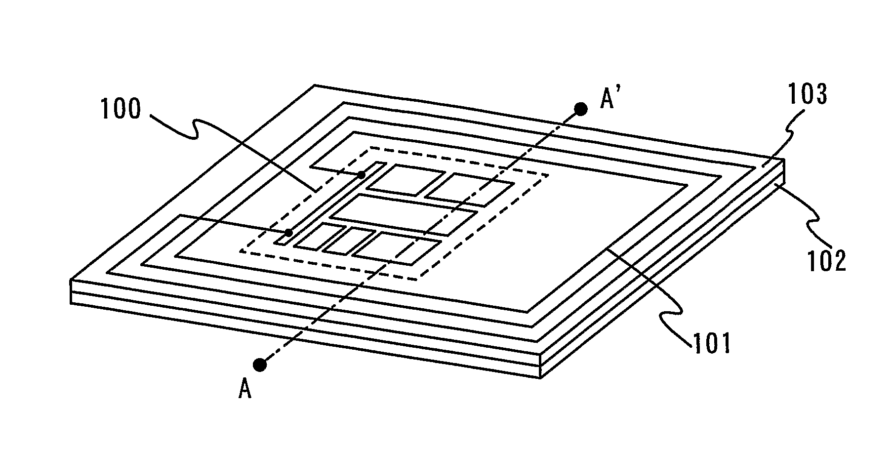
Semiconductor device
a technology of semiconductor substrate and barrier film, which is applied in the direction of shielding material radiating elements, semiconductor/solid-state device details, instruments, etc., can solve the problems of contaminated semiconductor elements, hardly improved reliability of id chips, and lower mechanical strength of semiconductor substrates than those of above magnetic cards and bar codes, so as to suppress stress per sheet of barrier films, and increase the thickness of barrier films
- Summary
- Abstract
- Description
- Claims
- Application Information
AI Technical Summary
Benefits of technology
Problems solved by technology
Method used
Image

Examples
embodiment 1
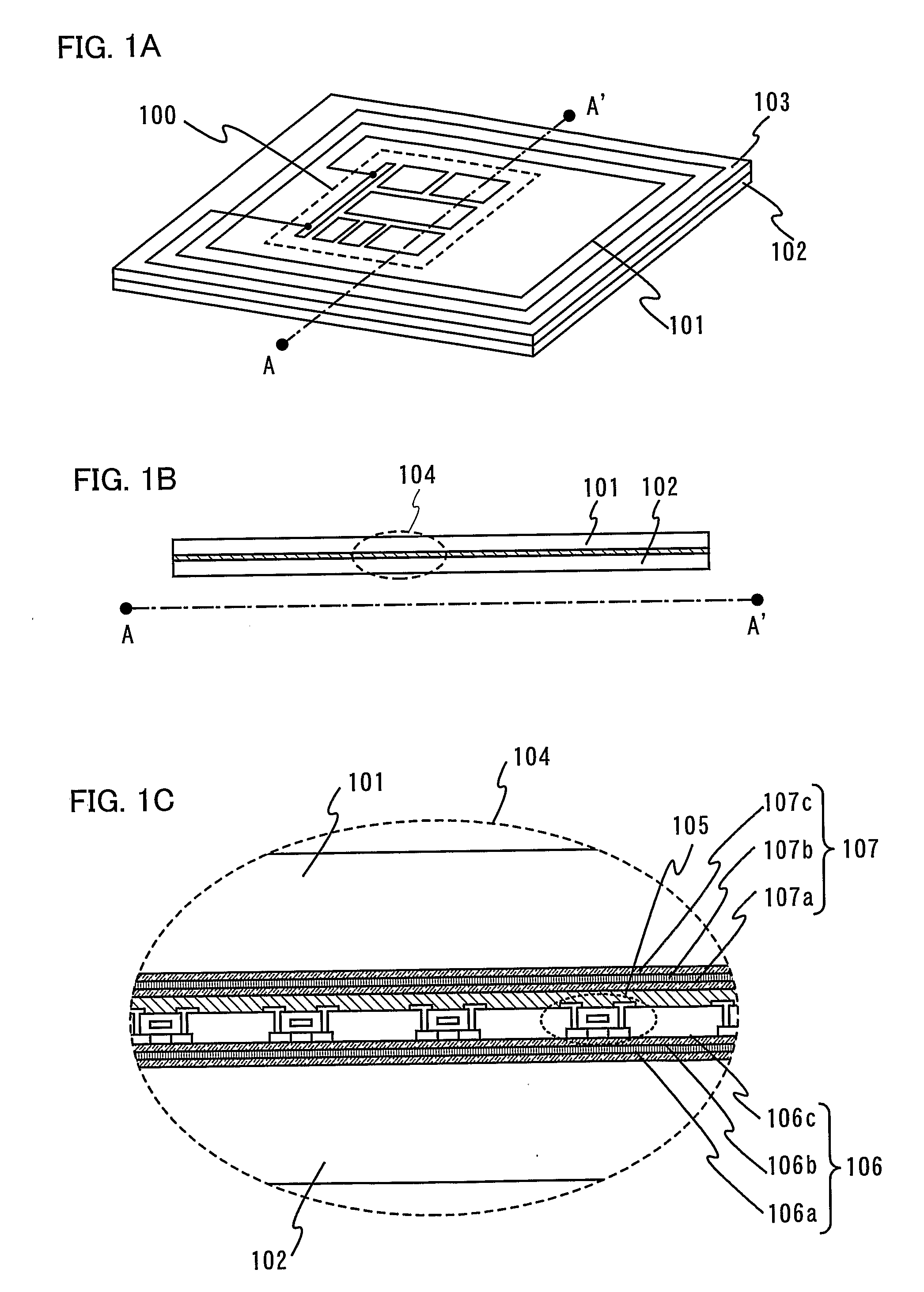
[0109] In the embodiment, a method for manufacturing an ID chip in which an antenna and an integrated circuit that are formed over different substrates are electrically connected to each other will be described, differing from FIGS. 2A to 2D, FIGS. 3A to 3C, and FIGS. 4A and 4B.
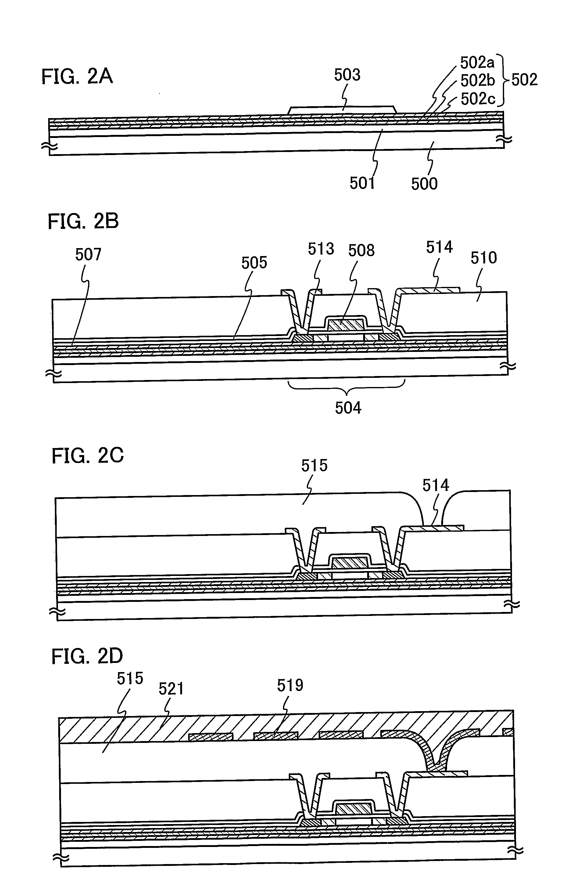
[0110] After forming the second interlayer insulating film 515 with an opening as shown in FIG. 2C, a wiring 550 connected to the wiring 514 is formed so as to be in contact with the second interlayer insulating film 515 as shown in FIG. 5A. A protective layer 551 is formed over the second interlayer insulating film 515 so as to cover the wiring 550. The structure and the manufacturing method of the protective layer 551 can refer the descriptions with respect to the protective layer 521 as shown in FIG. 2D.
[0111] A groove 552 is next formed to separate the ID chips one anotheL As shown in FIG. 5B, the separation layer 501 is removed by etching. The specific method for forming the groove 552 and the concrete...
embodiment 2
[0123] A structure of an ID chip in the case of forming a wiring connected to a TFT and an antenna by patterning one conductive film will be explained. FIG. 6A is a cross sectional view of the ID chip according to the present embodiment.
[0124] In FIG. 6A, reference numeral 601 denotes a TFT. The TFT 601 includes a semiconductor film 602, a gate insulating film 603 for covering the semiconductor film 602 and a gate electrode 604 that overlaps with the semiconductor film 602 while sandwiching the gate insulating film 603 therebetween. The TFT 601 is covered with a passivation film 605 and a first interlayer insulating film 606. A wiring 607 formed on the first interlayer insulating film 606 is connected to the semiconductor film 602 via the gate insulating film 603, the passivation film 605 and the first interlayer insulating film 606.
[0125] An antenna 608 is formed on the first interlayer insulating film 606. The wiring 607 and the antenna 608 can be made together by forming a cond...
embodiment 3
[0126] A structure of an ID chip in the case of forming a gate electrode of a TFT along with an antenna by patterning one conductive film will be explained in the embodiment. FIG. 6B is a cross sectional view of the ID chip according to the present embodiment.
[0127] In FIG. 6B, reference numeral 611 denotes a TFT. The TFT 611 includes a semiconductor film 612, a gate insulating film 613 covering the semiconductor film 612 and a gate electrode 614 that overlaps with the semiconductor film 612 while sandwiching the gate insulating film 613 therebetween. An antenna 618 is formed on the gate insulating film 613. The gate electrode 614 and the antenna 618 can be made together by forming a conductive film on the gate insulating film 613 and patterning the conductive film into the respective patterns. By forming the antenna 618 and the gate electrode 614 together, the number of steps for manufacturing the ID chip can be reduced.
PUM
 Abstract
Description
Claims
Application Information