Semiconductor test system

a test system and semiconductor technology, applied in the direction of electronic circuit testing, measurement devices, instruments, etc., can solve the problems of difficult to perform highly accurate testing and increase the test cost, and achieve the effect of reducing the size of the apparatus, and reducing the amount of data

Inactive Publication Date: 2007-07-12
TEST RES LAB
View PDF3 Cites 12 Cited by
  • Summary
  • Abstract
  • Description
  • Claims
  • Application Information

AI Technical Summary

Benefits of technology

[0021] According to the thus configured present invention, since the digital signals outputted from the plurality of output terminals are T / D converted and averaged in an early stage after the T / D conversion to reduce the amount of data, a large number of parallel transportation paths and processing circuits are not required, allowing reduction in the size of the apparatus. Furthermore, the reduced amount of data allows improved throughput, faster processing and significant reduction in test time. Moreover, since data sampled multiple times are averaged and calibrated for the following pass / fail judgment, the effects of random noise and systematic noise superimposed on the data are reduced, allowing high accuracy testing.

Problems solved by technology

This requires longer test time than simultaneously measuring all output values, disadvantageously resulting in corresponding increased test cost.
Furthermore, when the technology described in Japanese Patent No. 3199827 is used, the output signal from the test terminal is an analog signal, so that noise components are easily superimposed on the output signal and it is hence difficult to perform highly accurate testing.

Method used


Image

  • Semiconductor test system
  • Semiconductor test system
  • Semiconductor test system

Examples


first embodiment

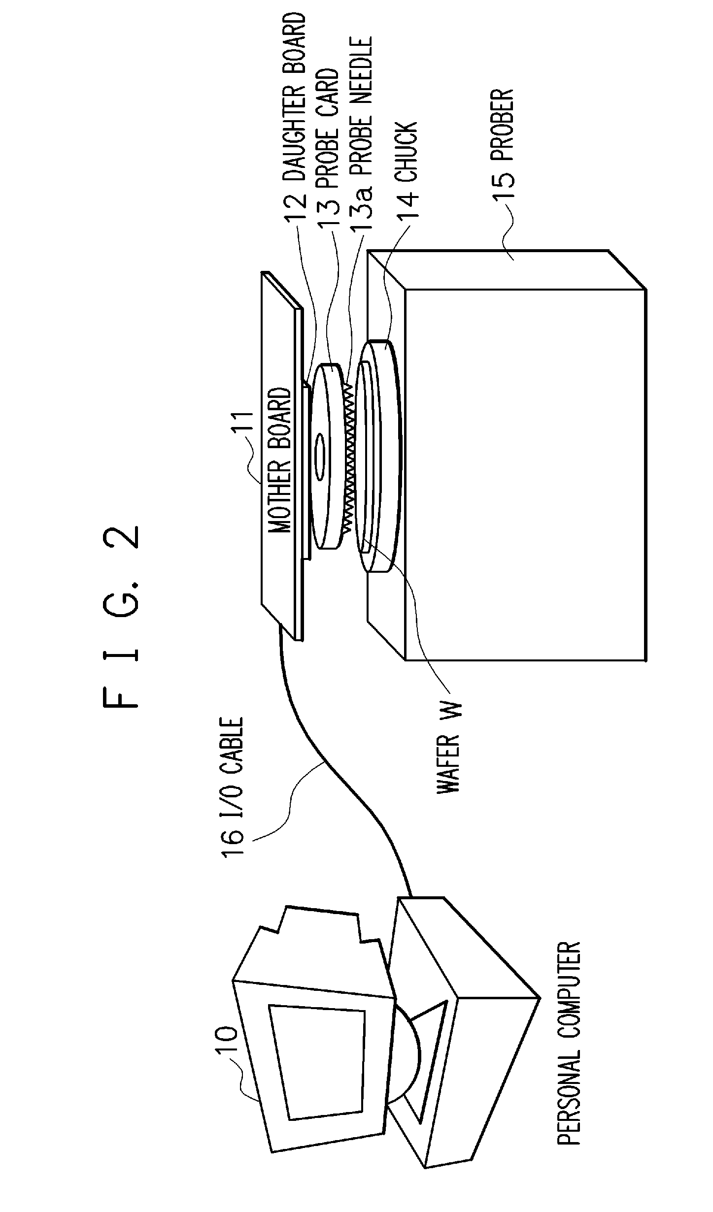
[0030] A first embodiment according to the present invention will be described below with reference to the drawings. FIG. 2 shows an exemplary schematic configuration of the entire test system according to the first embodiment. As shown in FIG. 2, the test system according to the first embodiment includes a personal computer 10, a mother board 11, a daughter board 12, a probe card 13, a chuck 14 and a prober 15. The probe card 13 has a plurality of probe needles 13a disposed thereon.

[0031] The wafer W to be tested is placed on the chuck 14 formed on the prober 15, and the probe needles 13a of the probe card 13 are moved to touch input / output terminals of an LSI formed on the wafer W. The probe card 13 is connected to the mother board 11 via the daughter board 12, and the mother board 11 is connected to the personal computer 10 via an I / O cable 16. Although the mother board 11 is directly connected to the personal computer 10 by the I / O cable 16 in this embodiment, the connection ma...

second embodiment

[0046] A second embodiment of the present invention will be described below with reference to the drawings. The whole configuration of the test system according to the second embodiment is the same as that shown in FIG. 2.

[0047]FIG. 5 is a block diagram showing an exemplary inner configuration of the mother board 11 and the daughter board 12 according to the second embodiment. In FIG. 5, since the components having the same reference characters as those shown in FIG. 3 have the same functions, redundant description thereof will be omitted.

[0048] As shown in FIG. 5, the mother board 11 according to the second embodiment includes a secondary judgment processor 23 instead of the judgment processor 22 shown in FIG. 3. The daughter board 12 according to the second embodiment further includes a primary judgment processor 36 between the calibration processor 34 and the digital interface 35.

[0049] The primary judgment processor 36 performs primary pass / fail judgment on the digital data c...

third embodiment

[0053] A third embodiment of the present invention will be described below with reference to the drawings. In the first and second embodiments described above, the voltage values outputted from the analog output terminals after test data are inputted to the LSI to be tested are used as reference values to test the LSI. In contrast, in the third embodiment that will be described below, temporal shifts (such as response time) of digital data outputted from digital output terminals after pulse-like digital data are inputted to the LSI are used as reference values to test the LSI (so-called timing test).

[0054] The whole configuration of the test system according to the third embodiment is the same as that shown in FIG. 2. FIG. 6 is a block diagram showing an exemplary inner configuration of the mother board 11 and the daughter board 12 according to the third embodiment.

[0055] As shown in FIG. 6, the mother board 11 according to the third embodiment includes a timing generator 41, a sw...


PUM


Abstract

There are included a mother board (11), which has therein a multiplexer and a test pass/fail determining part, and a daughter board (12) that has therein an A/D converting part and an averaging part. The mother board (11) multiplexes a plurality of analog signals outputted from a plurality of output terminals of an LSI formed on a wafer (W) to be tested, thereby reducing the number of signals in an early stage. The daughter board (12) A/D converts and averages the resultant signals from the mother board (11), and supplies the averaged characteristic measured data to the mother board (11) for a pass/fail determination. This can eliminate the need for a large number of parallel transmission paths and processing circuits, raise the throughput, and reduce the affections of noise included in the analog signals due to the average processing.

Description

CROSS REFERENCE TO RELATED APPLICATIONS [0001] This application is a Continuation of International Application PCT / JP2004 / 012693 filed on Aug. 26, 2004, the entire contents of which are incorporated herein by reference.BACKGROUND [0002] 1. Technical Field [0003] The present invention relates to a semiconductor test system. Particularly, the present invention is suitably applied to a test system for testing electric characteristics of a super multi-pin output LSI. [0004] 2. Background Art [0005] In display apparatuses, such as liquid crystal displays, organic EL displays, plasma displays and field emission displays, image data are processed in an electronic circuit, such as a drive circuit, and outputted from a plurality of output terminals of the drive circuit to display elements. Since the electric characteristics of drive transistors disposed corresponding to the output terminals of the drive circuit and components of the electronic circuit vary to no small extent, the signal valu...

Claims


Application Information

Patent Timeline
Patent Type & Authority Applications(United States)
IPC IPC(8): G01R31/28
CPCG01R31/2831
Inventor TANAKA, YOSHITO
Owner TEST RES LAB
Why Eureka
Try Eureka