Semiconductor package structure and fabrication method thereof

a technology of semiconductors and packaging, applied in the direction of semiconductor devices, semiconductor/solid-state device details, electrical apparatus, etc., can solve the problems of serious limitation, package structure cannot be stacked to increase the overall electrical performance, and is not suitable for packaging haring chip bond pads, etc., to improve the overall electrical functionality and performance of the package, compact and thin structure, easy to stack

Inactive Publication Date: 2007-07-19
SILICONWARE PRECISION IND CO LTD
View PDF7 Cites 36 Cited by
  • Summary
  • Abstract
  • Description
  • Claims
  • Application Information

AI Technical Summary

Benefits of technology

[0021]Moreover, in the semiconductor package of the invention, passive components can be also included attached to the substrate, so as to improve the overall electrical functionality and performance of the package.
[0022]In comparison with the conventional technology, the semiconductor package of the invention and the fabricating method th...

Problems solved by technology

One problem with the foregoing semiconductor package is that the leads must be protruded from the encapsulant to be able to electrically connect the package to an external device such as printed circuit board, and this protruding design will occupy a relatively large area of the printed circuit board compared to the overall package size.
However, facing the challenging demands of multi-functional electronic products, the foregoing package structure cannot be stacked to increase the overall electrical performance, and thus is inherent with a serious limitation.
It is not that suitable for packages haring a chip's bond pads employing cross-type, I-type...

Method used


Image

  • Semiconductor package structure and fabrication method thereof
  • Semiconductor package structure and fabrication method thereof
  • Semiconductor package structure and fabrication method thereof

Examples


first preferred embodiment

[0040]Referring to FIGS. 5A to 5E, top and cross-sectional views of the semiconductor package of the invention and the fabricating method thereof are shown.

[0041]The first embodiment of the invention is carried out in batches (hence the array of substrate modules 54A in FIG. 5A), so as to increase fabrication yield, however it can also be carried out as a single fabrication.

[0042]As shown in FIG. 5A, a substrate module 54A having a plurality of substrates 54 is provided. Each of the substrates 54 has at least one opening 541 and the arrangement of the opening 541 is based on the arrangement of bond pads disposed on the active surface of the semiconductor chip. In the present embodiment, as the bond pads on the active surface of the semiconductor chip are arranged in an I-shape, the corresponding opening 541 is an I-shaped opening. In addition, a plurality of electrical connection pads 542 and conductive circuits 543 are formed on the substrate 54 to provide electrical connections fo...

second preferred embodiment

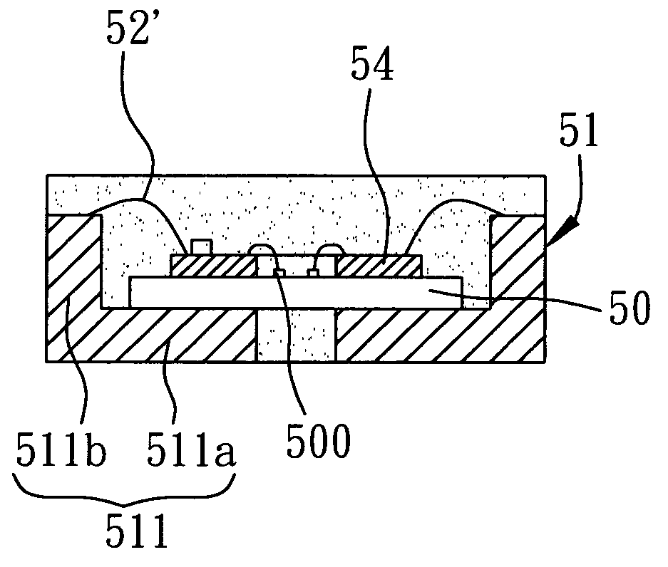
[0049]Referring to FIG. 6A, a leadframe 51 having a plurality of leads 511 is provided. Each lead 511 has an inner portion 511a and an outer portion 511b that are formed with differing heights. The height of the outer portion 511b of each lead 511 is larger than the height of the inner portion 511a of each lead 511, wherein the semiconductor chip 50 is attached to the inner portions 5111a of the leads 511. The semiconductor chip 50 has an active surface 50a and an opposing non-active surface 50b, and is attached to the inner portion 511a of the leads 511 via its non-active surface 50b. Also, the active surface 50a of the semiconductor chip 50 has bond pads 500 disposed thereon.

[0050]As shown in FIG. 6B, the active surface 50a of the semiconductor chip is attached to the substrate 54. The substrate 54 has an opening 541 at a position based on the arrangement of the bond pads 500 disposed on the active surface 50a of the semiconductor chip 50, allowing the bond pads 500 to be exposed ...

third preferred embodiment

[0054]As shown in FIG. 7, a cross-sectional view of the semiconductor package of the third preferred embodiment of the invention is shown.

[0055]The third preferred embodiment of the invention is almost the same as the forgoing first preferred embodiment. The major difference is that, in the present embodiment, the size of the substrate 54 is larger than the size of the semiconductor chip 50, but, as before, the semiconductor chip 50 is attached to the inner portion 511a of each of the leads 511, while the substrate 54 is attached on the semiconductor chip 50 and is electrically connected to the inner portions 511a of the leads 511 of the leadframe 51.


PUM


Abstract

A semiconductor package structure and a fabrication method thereof are provided. A semiconductor chip having an active surface and an inactive surface is coupled to a substrate. A plurality of bond pads are formed on the active surface of the semiconductor chip. The substrate can be arranged to expose the bond pads. The semiconductor chip is further attached to a lead frame having a plurality of leads, each of which has an inner portion and an outer portion higher than the inner portion, such that the semiconductor chip can be accommodated in the inner portions of the leads. An encapsulant is formed to cover the semiconductor chip and the substrate, and bottom surfaces of the leads of the lead frame are exposed from the encapsulant, so as to form a thin and compact package structure, which can package various semiconductor chips having different arrangements of bond pads.

Description

FIELD OF THE INVENTION[0001]The present invention relates to semiconductor packages and fabricating methods thereof, and more particularly to a leadframe-based semiconductor package and a fabrication method thereof.BACKGROUND OF THE INVENTION[0002]Conventionally, a thin small outline package (TSOP) is formed by attaching a semiconductor chip to a leadframe having a plurality of leads on its two sides and then forming an encapsulant to encapsulate the semiconductor chip and utilizing the leads on the two sides of the leadframe to electrically connect the chip to an external device.[0003]A cross-sectional schematic view of a conventional TSOP is shown in FIG. 1, comprising a leadframe 11 having a die pad 111 and a plurality of leads 112 on two sides of the die pad 111; a semiconductor chip 10 electrically connected to the leads 112 via bonding wires 12; and an encapsulant 13 for encapsulating the chip 10, bonding wires and part of the leads 112. The semiconductor chip 10 is electrical...

Claims


Application Information

Patent Timeline
IPC IPC(8): H01L23/495
CPCH01L21/561H01L24/48H01L23/3135H01L23/49531H01L23/49551H01L24/97H01L25/105H01L2224/48091H01L2224/4824H01L2224/48247H01L2224/48257H01L2224/4826H01L2224/4911H01L2224/73215H01L2224/97H01L2924/01082H01L2924/19041H01L2924/19106H01L2924/19107H01L23/3107H01L2224/32245H01L2225/1058H01L2225/1041H01L2225/1029H01L2924/01033H01L24/49H01L2924/00014H01L2224/85H01L2224/83H01L2924/00012H01L2924/181H01L2224/45099H01L2224/45015H01L2924/207
Inventor HUANG, CHIEN-PINGCHANG, CHIN-HUANG
Owner SILICONWARE PRECISION IND CO LTD
Why Eureka
Try Eureka