Pattern forming method and its mold

a technology of pattern forming and mold, applied in the field of pattern forming methods, can solve the problems of reducing alignment accuracy, difficult to align accurately and repeatedly, and achieving high precision alignmen

Inactive Publication Date: 2007-07-19
HITACHI LTD
View PDF4 Cites 23 Cited by
  • Summary
  • Abstract
  • Description
  • Claims
  • Application Information

AI Technical Summary

Benefits of technology

[0015]The present invention is intended to provide a pattern forming method capable of carrying out a high precision alignment between a disc substrate in which a hole is formed in the center of the substrate, and a mold in forming a fine pattern structure using a nano imprint technique.
[0018]In forming a fine pattern structure using a nano imprint technique, use of the present invention may provide a pattern forming method capable of carrying out a high precision alignment between a disc substrate, in which a hole is formed in the center of the substrate, and a mold regardless of whether or not an alignment mark at the time of contacting has a damage.

Problems solved by technology

Moreover, the hole diameter of the center of the disc substrate also varies due to errors at the time of machining, and therefore, in carrying out alignment between the mold and the disc substrate only using the projection, the alignment accuracy will vary for each disc substrate to use and it is thus difficult to align accurately and repeatedly.
In the method of JP-A-2001-325725, because the master center and the central opening of the disc substrate are shot at the same time, the resolution is unlikely to be obtained, resulting in decrease in the alignment accuracy.
As described above, there is a problem that a precise alignment between the substrate, in which an opening is formed in the center like a disc substrate, and a mold is difficult.

Method used


Image

  • Pattern forming method and its mold
  • Pattern forming method and its mold
  • Pattern forming method and its mold

Examples


embodiment 1

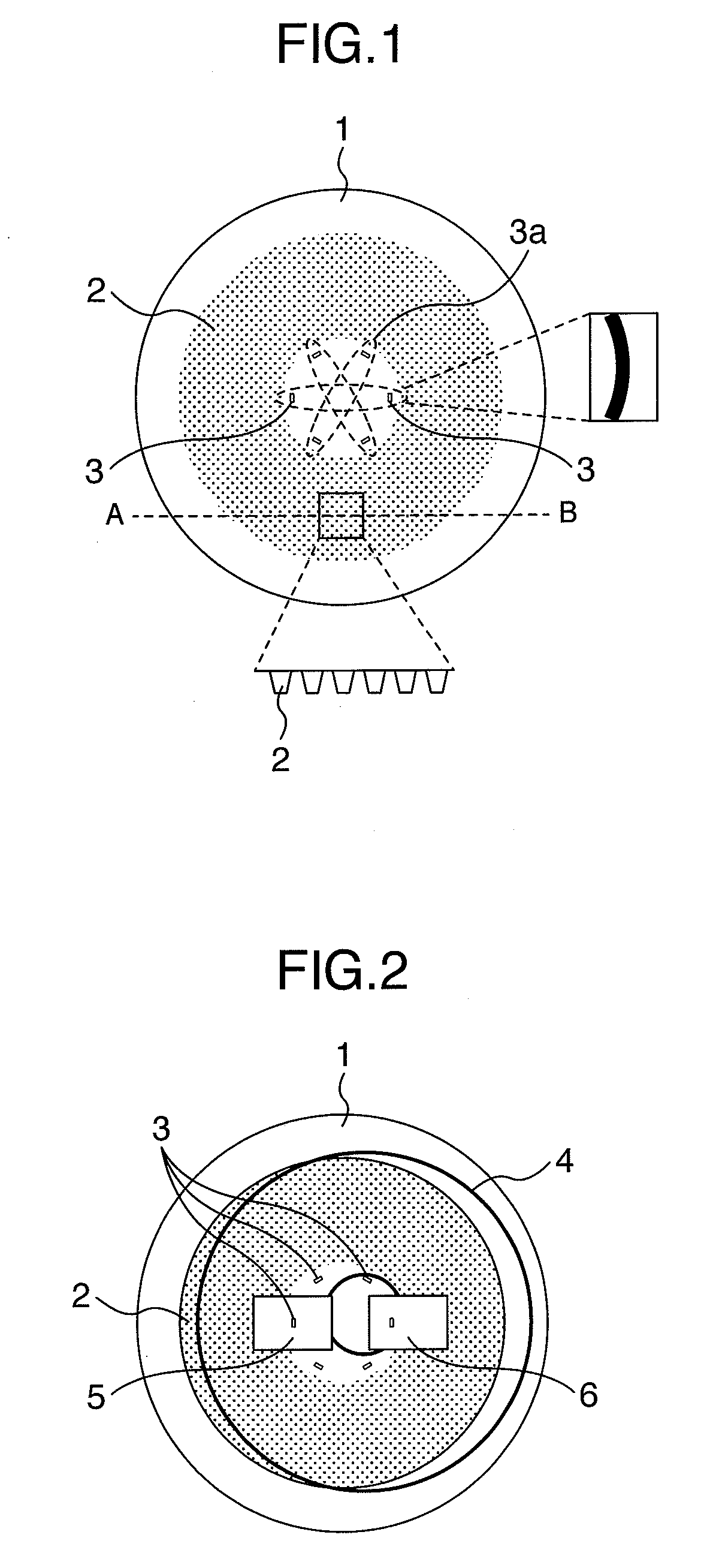
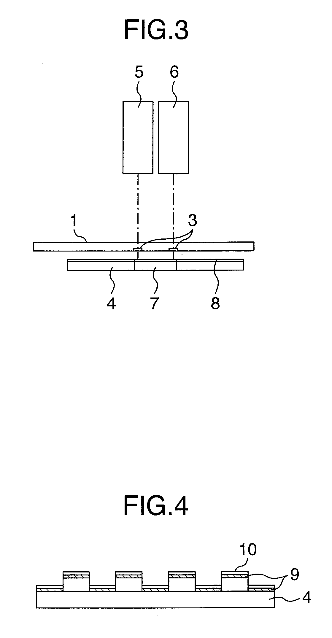
[0046]FIG. 1 shows a top view of a mold 1 used in this embodiment. The mold 1 is made of a quartz substrate and is a disc with 1000 μm in thickness and 100 mm in diameter. A fine concavo-convex pattern 2 of 100 nm or less may be easily processed on the surface of the mold 1 using a well-known electron beam drawing technique.

[0047]The fine concavo-convex pattern 2 formed in the surface of the mold 1 is arranged on circumferences concentric to the center opening of the disc substrate. This concavo-convex pattern 2 is prepared as follows: first, a resist pattern is formed patterning a resist layer formed on the substrate by means of the electron beam drawing technique, and then, concave portions are formed on the mold 1 using the resist pattern as a mask by means of a well-known dry etching technique. The concavo-convex pattern 2 prepared here has a via structure having the cross section with 35 nm in diameter at the concave upper surface, 20 nm in diameter at the concave bottom surfac...

embodiment 2

[0063]A mold is prepared using the same method as that of Embodiment 1. In the concavo-convex pattern prepared here, a columnar structure having the cross section with 35 nm in diameter at the bottom surface, 20 nm in diameter at the upper surface, and 100 nm in depth, is arranged at intervals of 40 nm from pattern center to pattern center. Moreover, an alignment mark similar to that of Embodiment 1 is also formed.

[0064]For the disc substrate, a glass substrate manufactured and sold for recording media, the glass substrate being processed into 0.8 mm in thickness, 65 mm in diameter of the outer circle, and 20 mm in diameter of the center opening, is used.

[0065]The aligning method between the mold and the disc substrate, and a subsequent method of transferring a concavo-convex pattern to a resist layer which is applied to a recording surface of the disc substrate are carried out using the methods similar to those of Embodiment 1. With these methods, in the resin film is prepared a re...

embodiment 3

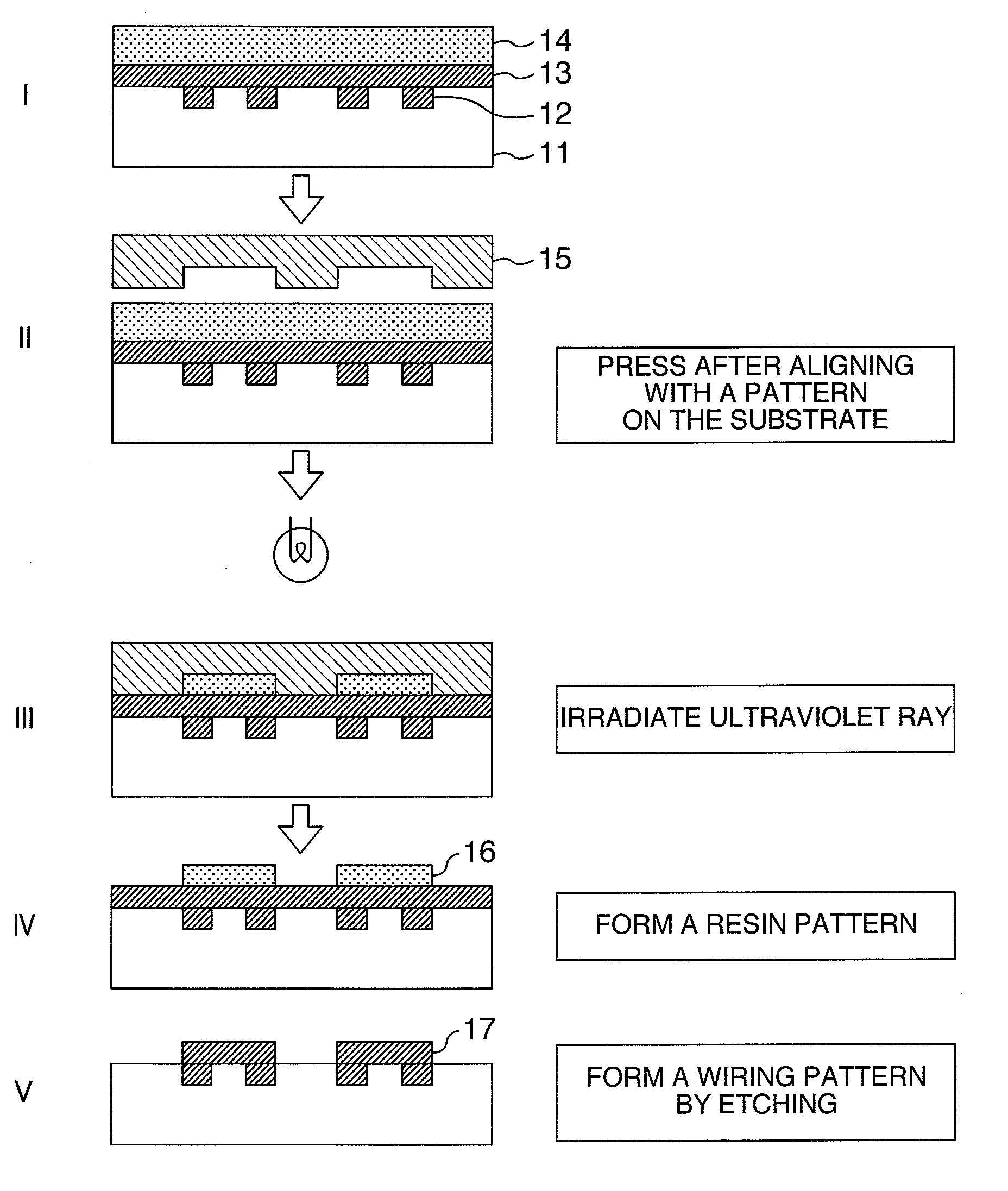
[0068]Next, a pattern forming procedure by nano imprint onto a silicon wafer is described using FIG. 6, which is a view schematically explaining a wiring pattern forming method in the case where a photo-curing type resin is used. A wiring pattern 12 is formed in a wafer 11. On this surface, an upper wiring layer 13 is deposited and a photo-curing type resin 14 is further applied (I). Next, a mold 15 in which a pattern is formed is brought closer to the wafer 11 from above the wafer 11, and after carrying out alignment between the mold 15 and the wafer 11 before contacting to each other, the both are relatively pressed to thereby form a pattern (II). The mold 15 is made of quartz and allows passage of light. By irradiating an ultraviolet ray from the back side of the mold 15 after pressing the mold 15, the concavo-convex pattern 2 of the resin film is cured (III). Removal of the mold 15 and removal of a base layer remaining at the bottom of the concavo pattern will form a resin patte...


PUM

PropertyMeasurementUnit
diameteraaaaaaaaaa
diameteraaaaaaaaaa
central angleaaaaaaaaaa

Abstract

In a mold in which a pattern is formed of a fine concavo-convex shape, two or more of alignment marks for determining a relative positional relation between a substrate and a mold are formed concentrically. Moreover, a damaged mark is identified from the positional information and shape of the respective marks, and an alignment between the mold and the substrate to which a resin film is applied is carried out excluding the damaged mark.

Description

BACKGROUND OF THE INVENTION[0001]1. Field of the Invention[0002]The present invention relates to a pattern forming method of transferring a fine concavo-convex pattern formed in a mold to a transferred substrate, and also relates to a mold using the same.[0003]2. Description of the Related Art[0004]In recent years, in integrated circuits the reduction in size and higher integration has been progressing, and as a pattern transfer technique for realizing this fine processing, higher precision of the photolithography apparatus has been pursued. However, the processing method is approaching the wavelength of a light source of light exposure and the lithography technology is also approaching the limit. For this reason, for pursuing further reduction in size and higher precision, an electron beam lithography apparatus which is a type of a charged particle beam apparatus is used in place of the lithography technology.[0005]The pattern formation using an electron beam employs a method of dr...

Claims


Application Information

Patent Timeline
Patent Type & Authority Applications(United States)
IPC IPC(8): H01L23/544H01L21/47B81C99/00
CPCB82Y10/00B82Y40/00G03F7/0002G03F9/7076G11B5/855H01L21/76838H01L2924/0002H01L23/544H01L2223/54453H01L2924/00
Inventor OGINO, MASAHIKOMIYAUCHI, AKIHIROANDO, TAKASHIHAGINOYA, CHISEKIKOMORIYA, SUSUMUSOHDA, YASUNARIKATAGIRI, SOUICHIOHTA, HIROYANAKAYAMA, YOSHINORI
Owner HITACHI LTD
Why Eureka
Try Eureka