Jitter detection and reduction

a jitter detection and reduction technology, applied in the field of jitter detection, can solve the problems of introducing jitter in the transfer process, and affecting the quality of signals produced by cdr circuits, so as to reduce jitter, reduce jitter in the output digital data signal, and reduce jitter

Inactive Publication Date: 2007-07-19
BOOKHAM TECH
View PDF5 Cites 6 Cited by
  • Summary
  • Abstract
  • Description
  • Claims
  • Application Information

AI Technical Summary

Benefits of technology

[0028]According to another aspect of the present invention, there is provided a method of reducing jitter in an output digital data signal generated by a clock and data recovery device from an input digital data signal and having a waveform defined by a plurality of component frequencies, including the steps of comparing a first indicator of the power of a selected frequency portion of the output digital data signal against a reference so as to provide a second indicator of the depth of a null in the frequency-power characteristic of the output data signal at a frequency equal to the data bit rate of the data signal or a multiple thereof.; and controlling the clock and data recovery device on the basis of the second indicator so as to reduce jitter in the output digital data signal.
[0029]Acco

Problems solved by technology

There is a problem that the signals produced by a CDR circuit can have “transfer jitter” introduced into them.
Transfer jitter is an unwanted variation in the timing of the signals, and is detrimental to the quality of the signals.
In particular, as the crossing point of the input signals goes below 50%, the jitter produced by the PLL of the CDR circuit increases.
The crossing po

Method used


Image

  • Jitter detection and reduction
  • Jitter detection and reduction
  • Jitter detection and reduction

Examples


first embodiment

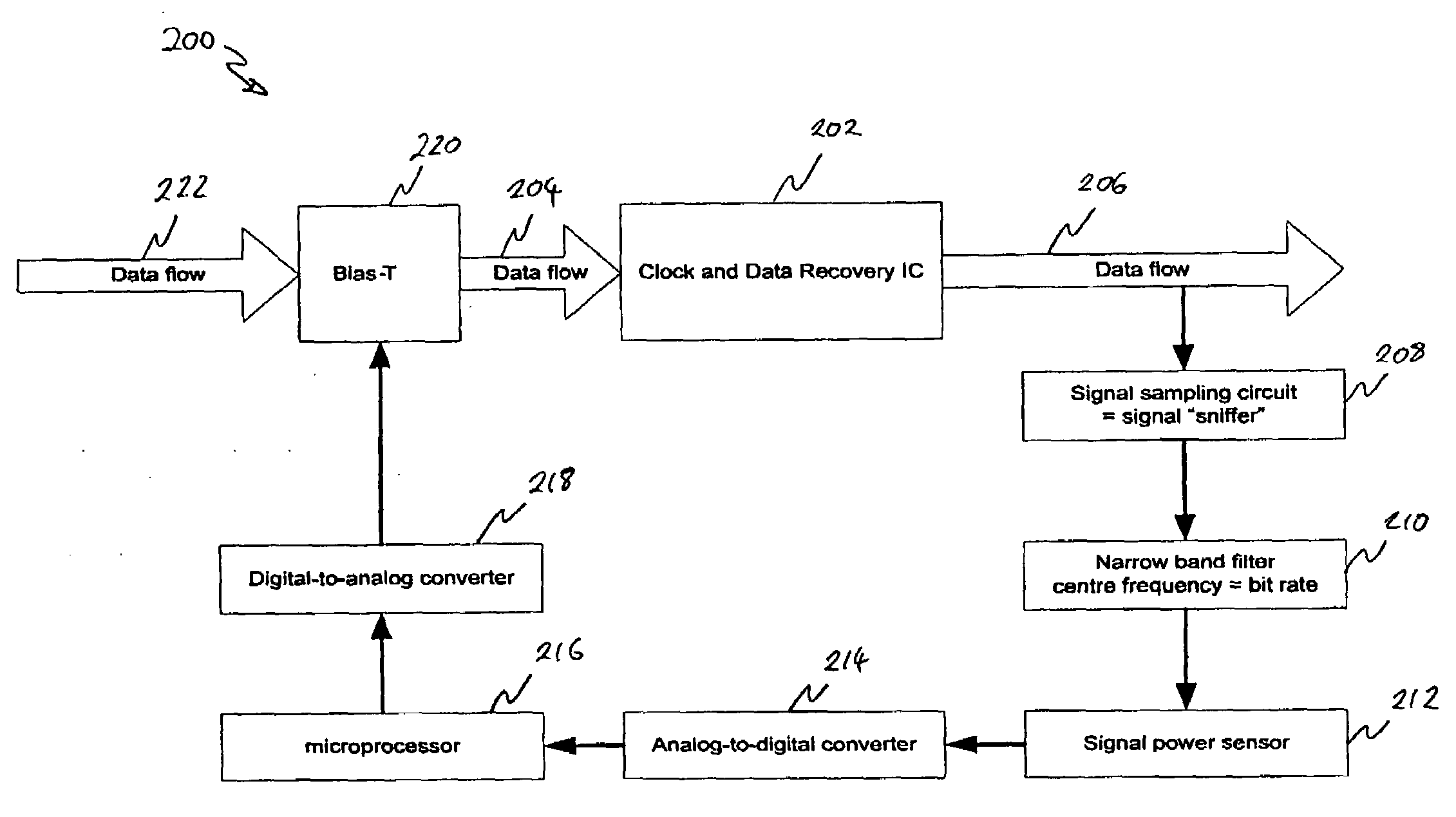
[0041]a system for utilising the above technique for detecting jitter can be seen with reference to FIG. 2. This figure shows a CDR system 200 for reducing the jitter present in the output signal by adapting a DC offset applied to the input signal.

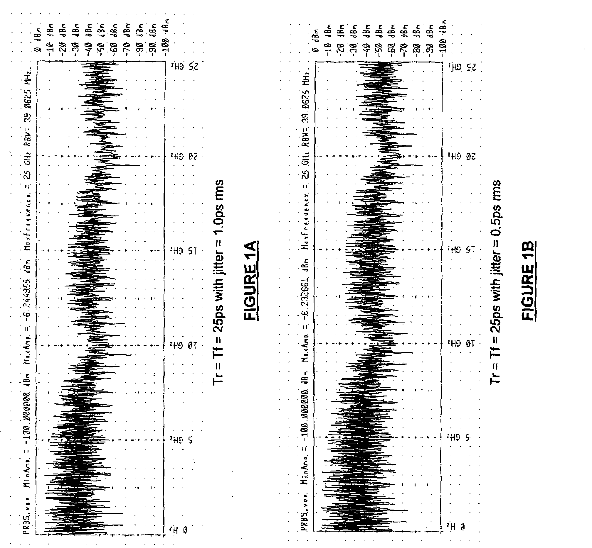
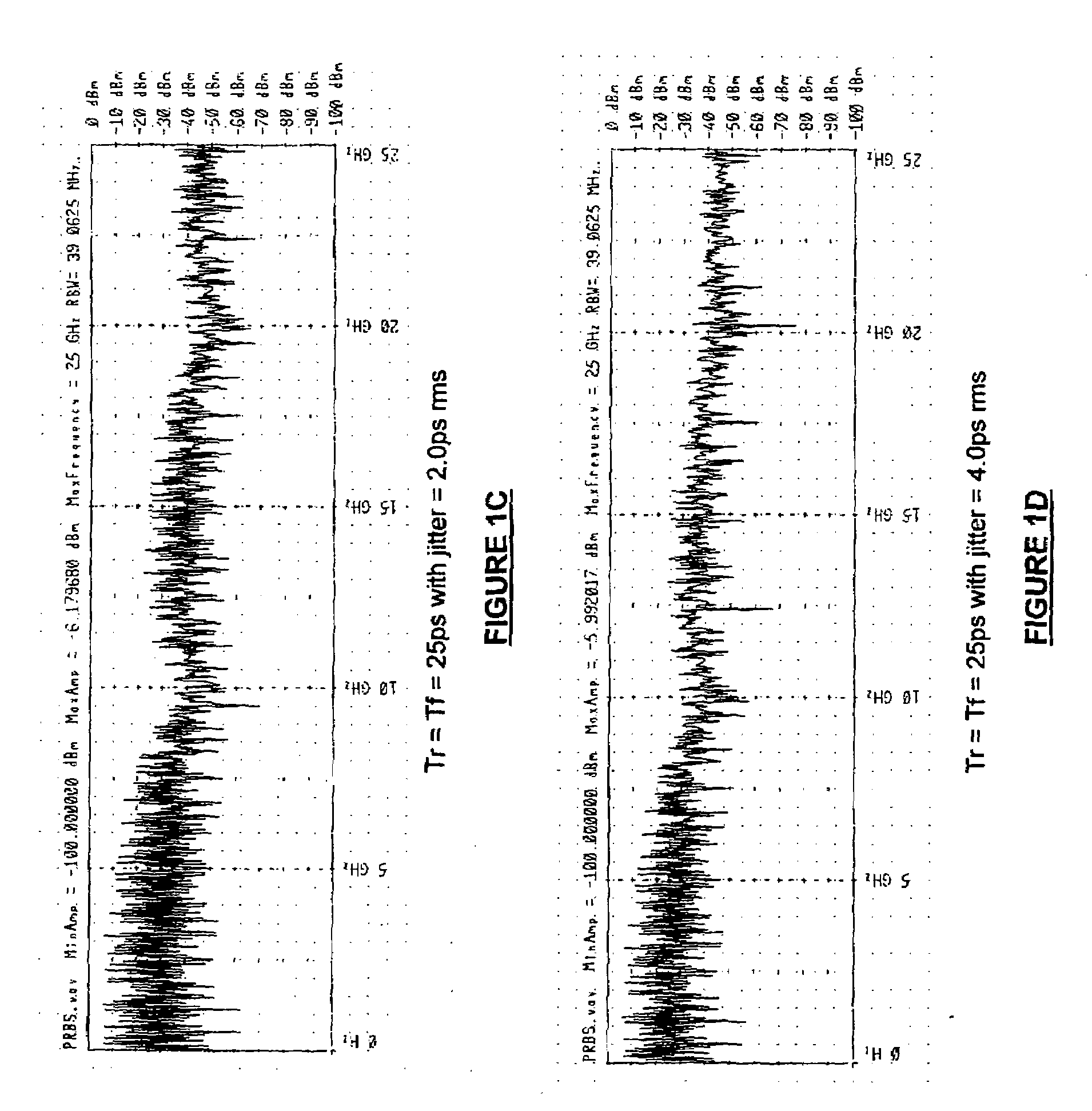
[0042]The system 200 comprises a CDR IC 202, which receives an input data signal 204, upon which a clock and data recovery process is performed to produce an output data signal 206. A signal sampling circuit 208 (also known as a signal “sniffer”) is used to extract a portion of the output signal 206 for processing. The signal from the sampling circuit 208 is passed through a narrowband filter 210. The centre frequency of the narrowband filter 210 is the bit rate of the input signal (or a multiple thereof, if an alternative null is being measured). Therefore, the narrowband filter 210 passes only the component frequencies that are present about the null shown above with reference to FIGS. 1a to 1d.

[0043]The narrowband filtered signal is pr...

second embodiment

[0046]the present invention is shown in FIG. 3. This figure shows a CDR system 300 with improved jitter determination. The system 300 in FIG. 3 comprises the same CDR IC 202 with a data signal input 204 and output 206 as shown previously in FIG. 2.

[0047]The output signal 206 is provided to a signal sampling circuit 302 which differs from that shown in FIG. 2 in that it produces two outputs. The first output is provided to a narrowband filter 210, signal power sensor 212 and ADC 214 in the same manner as described above with reference to FIG. 2 to provide a digital representation of the power at the null in the spectrum.

[0048]The second output of the signal sampling circuit 302 is provided to a wideband power sensor 304. The wideband power sensor 304 senses the power in the output signal over a much wider band than the power sensor 212. Typically, the wideband power sensor 304 senses the spectral power from a low frequency (LF) just above DC (i.e. close to 0 Hz) to just below the bit...

third embodiment

[0051]the present invention is shown in FIG. 4. This figure shows a CDR system 400 in which the jitter is minimised by controlling the loop bandwidth of the PLL 402 within the CDR IC 202.

[0052]In the embodiment shown in FIG. 4, the jitter is measured and determined in the same manner as described previously with reference to FIG. 3. Once the microprocessor 308 has determined the jitter it calculates an adjustment to be made to the loop bandwidth of the PLL 402 in order to minimise the jitter. The loop bandwidth of the PLL 402 is determined by the bandwidth of the loop filter. As mentioned previously, the bandwidth of the loop filter of the PLL 402 within the CDR IC 202 is controlled by the value of external components to the CDR IC 202, such as a resistor, a capacitor or a combination of a resistor and capacitor. The microprocessor determines the adjustment required to these external component values in order to achieve the required loop bandwidth to minimise the jitter.

[0053]The mi...


PUM


Abstract

A method of detecting jitter in a digital data signal having a waveform defined by a plurality of component frequencies, including the step of comparing an indicator of the power of a selected frequency portion of the digital data signal against a reference so as to provide an indicator of the shape of the frequency-power characteristic of the data signal.

Description

FIELD OF THE INVENTION [0001]The present invention relates to a technique for detecting jitter, and particularly but not exclusively for reducing jitter at a clock and data recovery device.BACKGROUND OF THE INVENTION [0002]Clock and data recovery (CDR) is an important part of a digital communication system. A clock and data recovery circuit allows a distorted digital signal to be re-timed, thereby providing cleaner and sharper data to following parts of the communication system.[0003]Clock and data recovery circuits are often used in optical communication systems. CDR circuits can be used in the transmitter of an optical system, for example between a terminal and a laser diode or electro-absorption modulator. CDR circuits are also used in the receiver of an optical system, such as between the line (optical fibre) side transimpedance amplifier (TIA) and the terminal.[0004]Known CDR circuits can be manufactured on a single integrated circuit (IC) for integration into a module of a com...

Claims


Application Information

Patent Timeline
IPC IPC(8): G06F19/00
CPCG01R31/31709
Inventor PAN, QIBARNARD, JOSEPH
Owner BOOKHAM TECH
Why Eureka
Try Eureka