Liquid phase epitaxial GOI photodiode with buried high resistivity germanium layer

a photodiode and liquid phase technology, applied in the field of integrated circuits, can solve the problems of poor ge crystallinity, leakage current, and inability to meet high-density large-scale commercial applications

Inactive Publication Date: 2007-07-26
SHARP LAB OF AMERICA INC
View PDF3 Cites 42 Cited by
  • Summary
  • Abstract
  • Description
  • Claims
  • Application Information

AI Technical Summary

Benefits of technology

[0007] The present invention provides a GOI structure to overcome the large dark current problem associated with poor Ge crystallinity at a Ge-to-insulator interface. The structure is a vertical P-I-N diode with p+-doped Ge-buried insulator interface. The perimeter of the diode is also doped p+. This structure eliminates Ge-buried insulator and lateral interface leakage current.

Problems solved by technology

However, the reported photodiode had a large dark current, and therefore, is not suitable for high-density large-scale commercial applications.
The leakage current is attributed to the poor Ge crystallinity at the Ge to insulator interface.

Method used


Image

  • Liquid phase epitaxial GOI photodiode with buried high resistivity germanium layer
  • Liquid phase epitaxial GOI photodiode with buried high resistivity germanium layer
  • Liquid phase epitaxial GOI photodiode with buried high resistivity germanium layer

Examples


Embodiment Construction

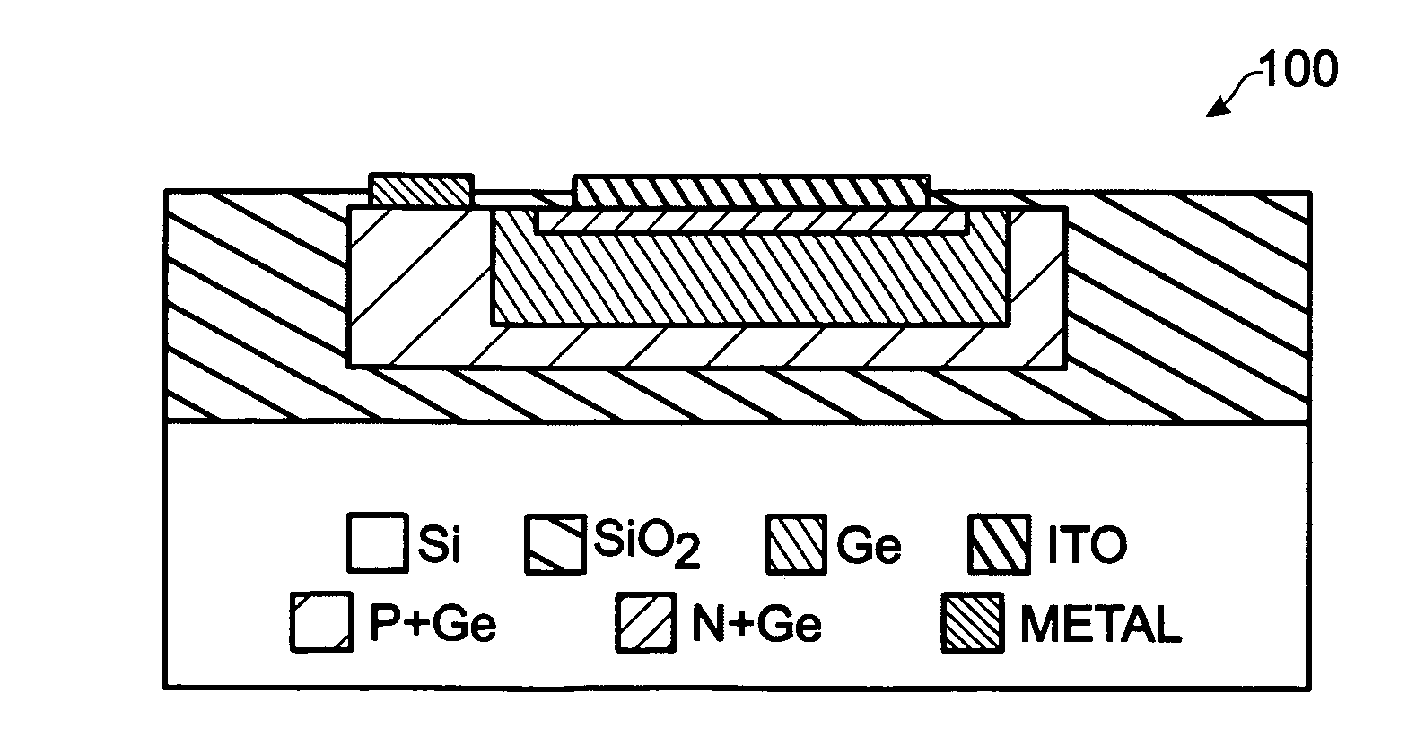
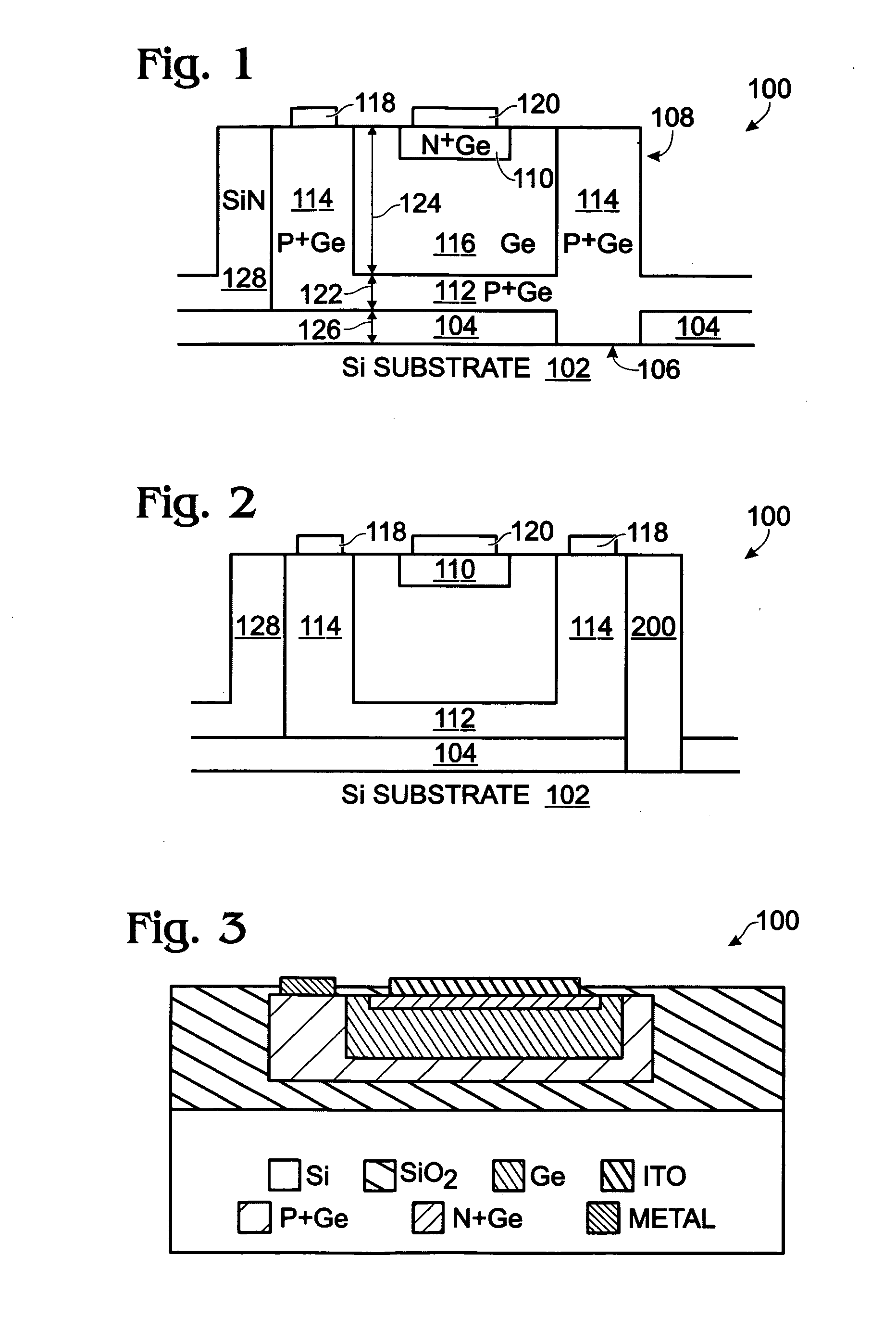
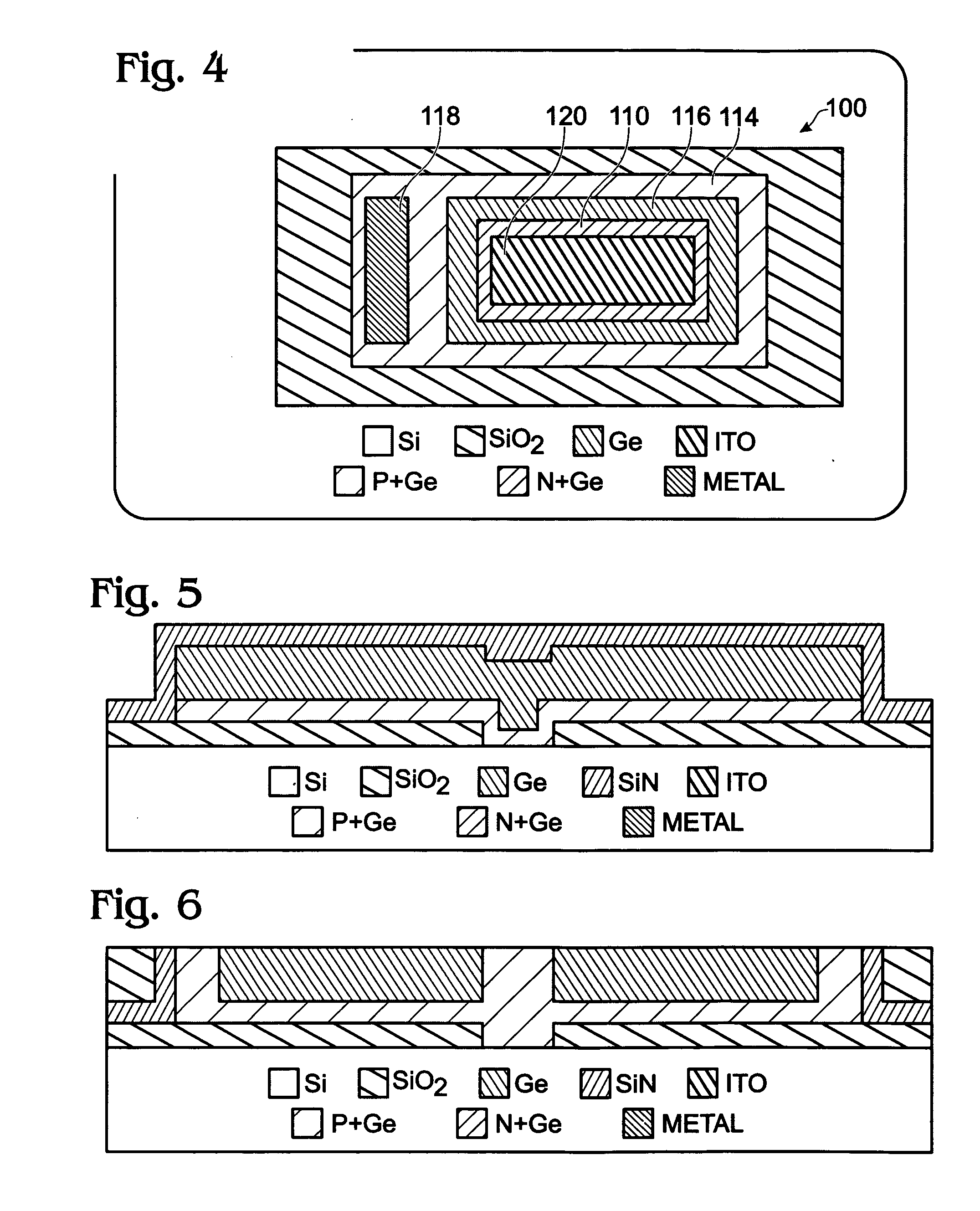
[0017]FIG. 1 is a partial cross-sectional view of a liquid phase epitaxial (LPE) Germanium-on-Insulator (GOI) photodiode with a buried high resistivity Germanium (Ge) layer. The photodiode 100 comprises a silicon (Si) substrate 102 and a bottom insulator 104 overlying the Si substrate 102 with a Si seed access area 106. Also shown is Ge P-I-N diode 108. The P-I-N diode 108 has an n+-doped (n+) mesa 110, a p+-doped (p+) Ge bottom insulator interface 112 and mesa lateral interface 114, and a high resistivity Ge layer 116 interposed between the p+ Ge 112 / 114 and n+ Ge 110. As seen more clearly in FIG. 4, the p+ Ge mesa lateral interface 114 forms a perimeter around the high resistivity Ge layer 116. A metal electrode 118 overlies a region of the p+ Ge mesa lateral interface 114. A transparent electrode 120 overlies the n+ Ge mesa 110. For example, the transparent electrode can be a conductive material such as ITO or a thin layer of Au.

[0018] In one aspect, the p+ Ge bottom insulator i...


PUM

PropertyMeasurementUnit
thicknessaaaaaaaaaa
thicknessaaaaaaaaaa
thicknessaaaaaaaaaa

Abstract

A device and associated method are provided for fabricating a liquid phase epitaxial (LPE) Germanium-on-Insulator (GOI) photodiode with buried high resistivity Germanium (Ge) layer. The method provides a silicon (Si) substrate, and forms a bottom insulator overlying the Si substrate with a Si seed access area. Then, a Ge P-I-N diode is formed with an n +-doped (n+) mesa, a p+-doped (p+) Ge bottom insulator interface and mesa lateral interface, and a high resistivity Ge layer interposed between the p+ Ge and n+ Ge. A metal electrode is formed overlying a region of the p+ Ge lateral interface, and a transparent electrode is formed overlying the n+ Ge mesa. In one aspect, the method deposits a silicon nitride layer temporary cap overlying the high resistivity Ge layer, and an annealing is performed to epitaxially crystallize the Ge bottom interface and high resistivity Ge layer.

Description

BACKGROUND OF THE INVENTION [0001] 1. Field of the Invention [0002] This invention generally relates to integrated circuit (IC) fabrication and, more particularly, a liquid phase epitaxial (LPE) Germanium-on-Insulator (GOI) photodiode with a buried high resistivity Germanium (Ge) layer. [0003] 2. Description of the Related Art [0004] A photodiode is a p-n junction receptive to optical input. Photodiodes can be either zero biased or reverse biased. If zero biased, light creates a current in the forward bias direction. This phenomena is called the photovoltaic effect. If reverse biased, photodiodes have a high resistance that is reduced when light is introduced to the p-n junction. A reverse biased diode is typically more sensitive to light, and can be used as a detector if the current flow is monitored. Phototransistors rely upon the p-n junction to detect light, but are typically more sensitve to light than a diode. [0005] There are many applications for photodetection in the near i...

Claims


Application Information

Patent Timeline
Patent Type & Authority Applications(United States)
IPC IPC(8): H01L31/00
CPCH01L31/1055Y02E10/50H01L31/1872H01L31/1808
Inventor HSU, SHENGLEE, JONG-JANMAA, JER-SHENTWEET, DOUGLAS
Owner SHARP LAB OF AMERICA INC
Why Eureka
Try Eureka