Double byte select high voltage line for EEPROM memory block

Inactive Publication Date: 2007-07-26
ATMEL CORP
View PDF12 Cites 22 Cited by
  • Summary
  • Abstract
  • Description
  • Claims
  • Application Information

AI Technical Summary

Benefits of technology

[0012] A byte select circuit of a memory cell array wherein each column of the memory cell array has two byte select lines. A first byte select line is coupled to the even numbered rows in the column and a second byte select line is coupled to the odd numbered rows in the column. The second byte select line is configured to be driven to a low voltage level when the first byte select line is driven to a high voltage level, thereby minimizing or eliminating any parasitic voltage coupling between adjacent rows of memory cells. In an exemplary embodiment, the present invention is a byte select circu

Problems solved by technology

Even though the length of the line from the source of, for example, the second byte select transistor 107 is very short, due to an extremely high packing density of transistors in integrated circuits, the

Method used


Image

  • Double byte select high voltage line for EEPROM memory block
  • Double byte select high voltage line for EEPROM memory block
  • Double byte select high voltage line for EEPROM memory block

Examples


Embodiment Construction

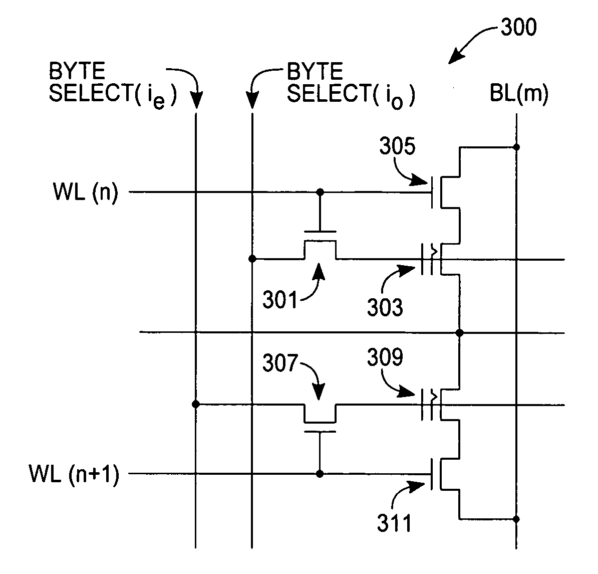
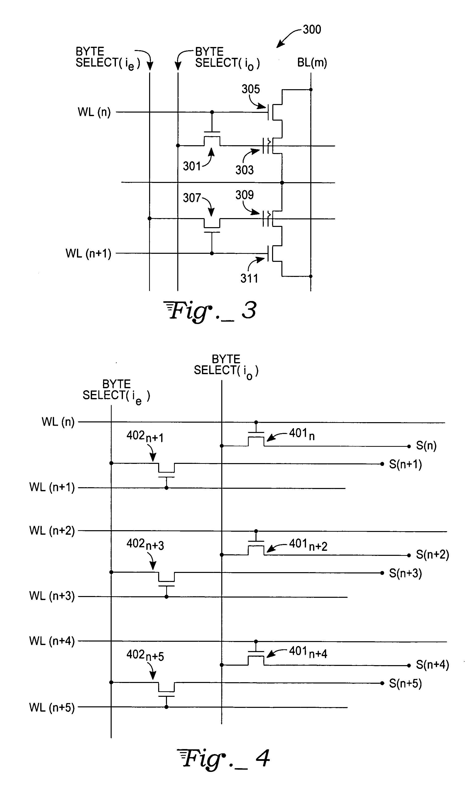
[0019] With reference to FIG. 3, a portion 300 of an exemplary embodiment of a memory array of the present invention includes a first byte select transistor 301 coupled to a gate of a first floating gate transistor 303. A first wordline, WL(n) is coupled to gates of both the first byte select transistor 301 and a bit select transistor 305. As with the prior art, an asserted high value (e.g., a logical “1”) on the wordline, WL(n) allows both the first byte select transistor 301 and the bit select transistor 305 to conduct, thereby allowing the first floating gate transistor 303 to be selected for read, write, or programming operations through a bitline, BL(m). The asserted high value on the wordline, WL(n), allows a source-drain current to flow from a byte select (io) line to a control gate of the first floating gate transistor 303. The byte select (io) line is also arranged with seven additional floating gate transistors (not shown) in parallel with the first floating gate transisto...


PUM


Abstract

A byte select circuit of a memory cell array wherein each column of the memory cell array has two byte select lines. A first byte select line is coupled to the even numbered rows in the column and a second byte select line is coupled to the odd numbered rows in the column. The second byte select line is configured to be driven to a low voltage level when the first byte select line is driven to a high voltage level, thereby minimizing or eliminating any parasitic voltage coupling between adjacent rows of memory cells.

Description

TECHNICAL FIELD [0001] The present invention relates generally to a non-volatile memory architecture. More specifically, the present invention is an EEPROM non-volatile memory architecture providing multiple byte select lines to alternating word line rows. BACKGROUND ART [0002] EEPROM arrays include floating-gate memory cells arranged in rows and columns. When a floating gate of a programmed memory cell is charged with electrons, a source-drain path under the charged floating gate is nonconductive when a wordline select voltage is applied to a control gate of the cell. A nonconductive state is read as a “1” bit. If the floating gate of a non-programmed cell is either positively charged, neutrally charged, or slightly negatively charged, the source-drain path under the non-programmed floating gate is conductive when the wordline select voltage is applied to the control gate. The conductive state is read as a “0” bit. [0003] In memories based on a Fowler-Nordheim tunneling mechanism, ...

Claims


Application Information

Patent Timeline
IPC IPC(8): G11C8/00
CPCG11C16/0433G11C16/3427G11C16/3418
Inventor LAMBRACHE, EMILCURRY, DUNCANPANG, RICHARD
Owner ATMEL CORP
Why Eureka
Try Eureka