Plasma Processing Apparatus And Method For Controlling The Same

a processing apparatus and plasma technology, applied in the field of semiconductor devices manufacturing, can solve the problems of not being able to guarantee the phase difference between the voltage actually appearing at the upper and lower electrodes, not being able to guarantee the phase difference of the voltage generated at the upper electrode as being controlled, and not being able to disclose the method of ensuring the achievement of the object by phase control, etc., to achieve the effect of high accuracy

Active Publication Date: 2007-09-13
HITACHI HIGH-TECH CORP
View PDF2 Cites 7 Cited by
  • Summary
  • Abstract
  • Description
  • Claims
  • Application Information

AI Technical Summary

Benefits of technology

[0020] In view of the problems mentioned above, the first object of the present invention is to provide a plasma processing apparatus and a method for controlling the plasma processing apparatus equipped with a function to utilize a most suitable signal for phase control, thereby solving drawbacks one through three mentioned above.
[0021] The second object of the present invention is to provide a plasma processing apparatus and a method for controlling the plasma processing apparatus equipped with the above function, that can be applied to a plasma source such as an inductively coupled plasma source having no two independent electrodes that are capacitively coupled with plasma, thereby solving the fourth drawback mentioned above.
[0023] Moreover, as a second actual example, with the object of suppressing sputtering and damage of the vacuum vessel wall and reducing the amount of contaminants caused thereby, a voltage probe is disposed around the target vacuum vessel to extract the RF signals transmitted from the upper and lower electrodes through plasma, and phase control is performed so as to minimize the voltage or to set the voltage to an appropriate value.
[0035] According to the present invention, upon performing phase control of the voltage waveforms of the third RF power and the second RF power supplying bias to the processing substrate, the phase difference at each electrode radiating power to the plasma can be controlled with high accuracy, and as a result of controlling the ion energy colliding against the wall and the interaction between ion and wall, the amount of substance generated from the wall can be controlled from minimum to maximum. As a result, it becomes possible to provide a most suitable in-vessel environment for each process performed in the apparatus for processing a processing substrate via plasma. Moreover, this function can be realized in all types of apparatuses that generate plasma, not only in those utilizing a parallel plate plasma source.

Problems solved by technology

However, according to the prior art, there are a means for detecting and a means for adjusting the phase difference of the RF between upper and lower biases, and though it is stated that the phase difference should preferably be controlled to 180 degrees, there is no disclosure on how to guarantee the achievement of the object by phase control.
The second drawback of the prior art is that even if the prior art method can be adopted to control the phase difference to 180 degrees, for example, it is not capable of guaranteeing that the phase difference of the voltages actually appearing at the upper and lower electrodes is 180 degrees.
Therefore, even if phase data is taken at each matching network of the upper and lower electrodes, the RF transmission paths that lead to the electrodes from the matching network vary, so there is no guarantee that the phase difference of the voltages generated at the electrodes is as controlled.
Another fact that influences the present problem is that the impedance of the RF transmission path leading to the earth seen from the upper electrode and the impedance of the RF transmission path leading to the earth seen from the lower electrode are not equal.
Further, since wafer processing is progressed near the lower electrode, the large amount of reaction products generated from the wafer causes the status of plasma near the lower electrode to change drastically.
What is concluded from the above is that the phase difference of voltages generated at upper and lower electrodes is determined by the overall circuits of RF passing the electrodes and the frequency of the RF, and therefore, it is not possible according to the prior-art monitoring method to accurately control the phase difference during wafer processing.
The third drawback of the conventional method results from the fact that the voltage waveform of RF biases generated at upper and lower electrodes is not a sine wave, and the conventional methods were incapable of performing optimum value control.
The cause of this displacement is that the phase difference of the electrodes are not performed accurately since the impedances of the RF transmission paths differ, and since the current / voltage waveform of the electrodes are deformed due to harmonics.
The fourth drawback of the conventional art is that the apparatus for improving wafer processing via phase control is restricted to a parallel plate plasma source equipped with upper and lower electrodes.
Various type of plasma sources are used in the industry such as an inductively coupled plasma source or an ECR plasma source, but the methods disclosed in the prior art cannot be applied to these plasma sources since they do not have two independent electrodes that are capacitively coupled with plasma.

Method used


Image

  • Plasma Processing Apparatus And Method For Controlling The Same
  • Plasma Processing Apparatus And Method For Controlling The Same
  • Plasma Processing Apparatus And Method For Controlling The Same

Examples


second embodiment

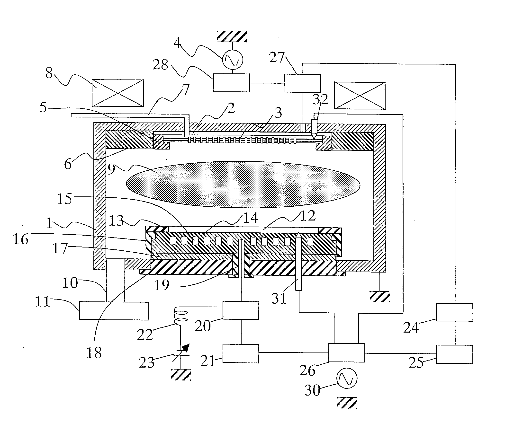
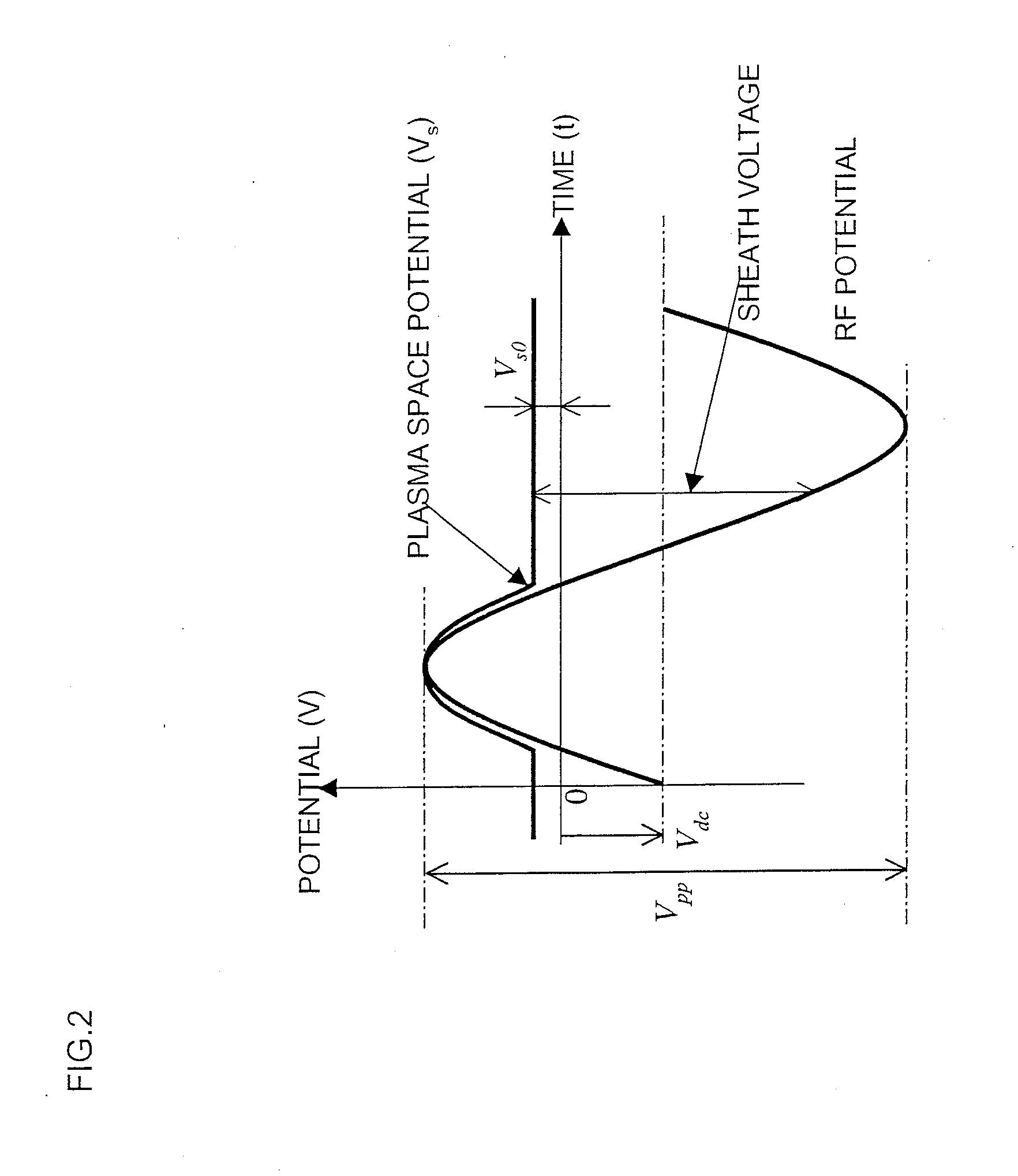
[0065] Based on the above fact, the present invention utilizes the RF transmitted in the plasma to perform phase control of the bias. In order to suppress the generation of contaminants, it is necessary to minimize the energy of ions accelerated toward the earth. Based on the above description, the conditions for realizing this is equal to that for minimizing the rise of plasma potential by the RF bias. the present invention utilizes these conditions, and the schematic view of this embodiment is illustrated in FIG. 3.

[0066] In this embodiment, a microelectrode 40 is inserted near the vacuum vessel wall, for receiving the RF transmitted through the plasma. The signal generated in the microelectrode 40 includes the RF from the first, second and third RF power supplies 4, 21 and 25 and their harmonics, the plasma floating potential and noise components. It is possible to use an analog filter or a digital filter (such as fast Fourier transform) in order to detect the RF from the second ...

third embodiment

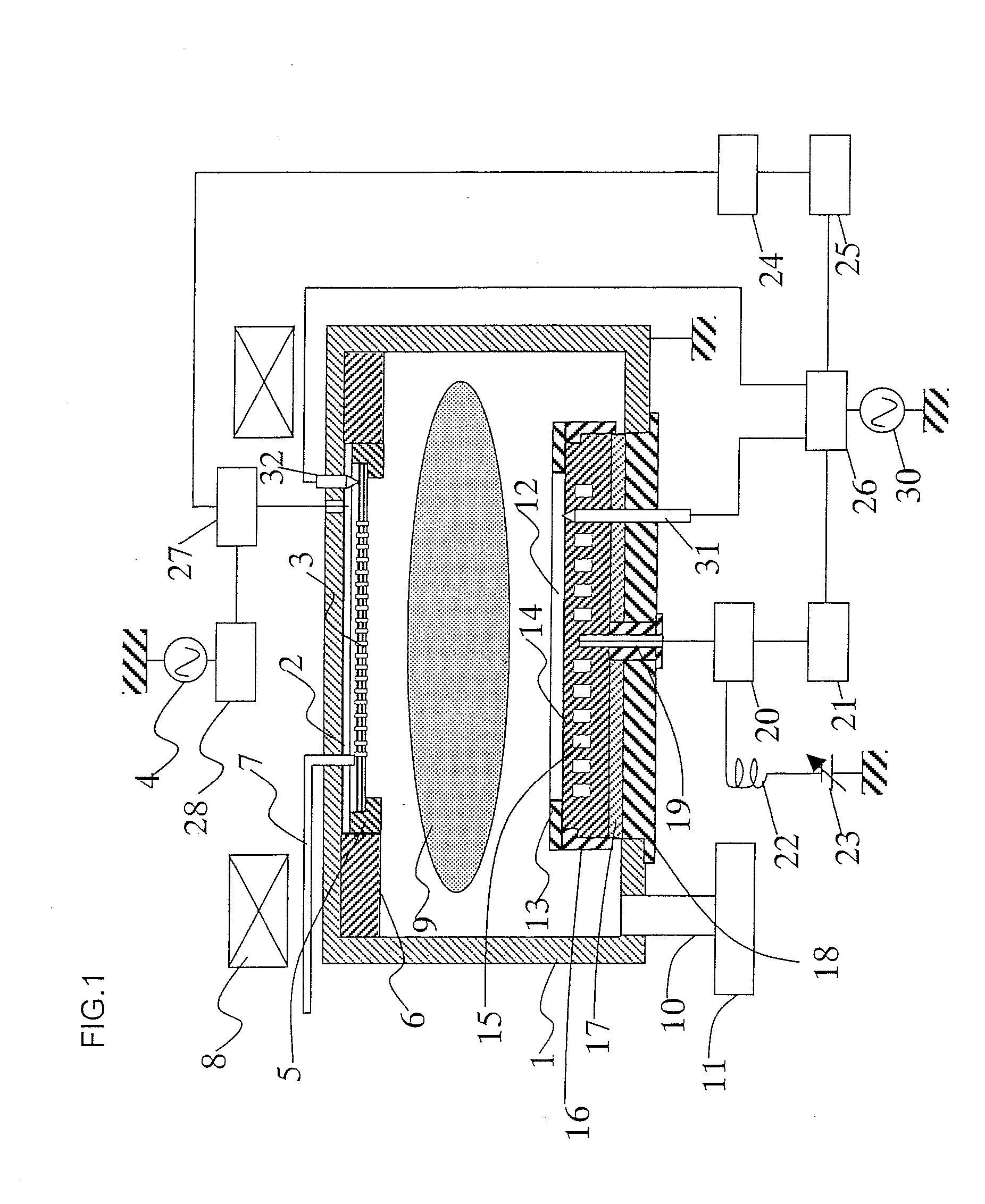
[0071] From the viewpoint of controlling the ion impact on the vacuum vessel wall, it is possible to adopt a means to detect the substances being released from the wall. the present invention is made from this viewpoint, and the schematic view thereof is illustrated in FIG. 5. The substance released from the wall is subjected to collisional excitation in the plasma by electrons, and emits light of a wavelength specific to that substance. By collecting this light through a window and a collimator lens 51 to a spectroscope 52, the intensity of the wavelength specific to the substance can be obtained at the spectroscope 52. The emission intensity is used as a control signal for controlling a phase controller 29.

[0072] The arrangement of FIG. 5 was used to generate oxygen plasma (electron density: approx. 3×1016 cm−3, electron temperature: approx. 2.5 eV). Using an aluminum having an alumite treated surface (anodized aluminum surface) as the vacuum vessel 1, the phase of the phase contr...


PUM

PropertyMeasurementUnit
diameteraaaaaaaaaa
frequencyaaaaaaaaaa
frequencyaaaaaaaaaa

Abstract

A method for controlling a plasma processing apparatus which includes a vacuum vessel, a first, second and third RF power supply, a first and second electrode, and a phase control unit for controlling a phase difference between a second RF voltage from the second RF power supply and a third RF voltage from the third RF power supply. The controlling method includes the steps of supplying a predetermined power from the first RF power supply to ignite plasma, after confirming ignition of plasma, supplying a predetermined power respectively from the second RF power supply and the third RF power supply, and when starting power supply from the second RF power supply and the third RF power supply, fixing the phase to a predetermined phase angle using a preset mode without carrying out phase control, and after a matching operation has stabilized, starting the phase control.

Description

CROSS REFERENCE TO RELATED APPLICATION [0001] This application is a divisional application of U.S. application Ser. No. 11 / 036,097, filed Jan. 18, 2005, the contents of which are incorporated herein by reference. [0002] The present application is based on and claims priority of Japanese patent application No. 2004-341723 filed on Nov. 26, 2004, the entire contents of which are hereby incorporated by reference.BACKGROUND OF THE INVENTION [0003] 1. Field of the Invention [0004] The present invention relates to an art for manufacturing semiconductor devices. Specifically, the present invention relates to a plasma processing apparatus and a method for controlling the plasma processing apparatus suitable for carrying out a plasma processing of a semiconductor wafer using plasma. [0005] 2. Description of the Related Art [0006] Along with the recent trend of large-scale integration of semiconductor devices, the circuit patterns have become finer and finer, and the demands for accurate dime...

Claims


Application Information

Patent Timeline
Patent Type & Authority Applications(United States)
IPC IPC(8): H01L21/306
CPCC23F4/00H01J37/32165H01J37/32082
Inventor NISHIO, RYOJI
Owner HITACHI HIGH-TECH CORP
Why Eureka
Try Eureka